Magnetoelectric flat band induced by a charge density wave in monolayer CrSe2
Abstract
We investigate the electronic and magnetic properties of the polar charge-density-wave (CDW) phase of CrSe2 using ab initio calculations. The CDW introduces a polar distortion out of the van der Waals plane that couples to the spin-polarized Cr d states resulting in a remarkably flat electronic band exactly at the Fermi level. We provide a microscopic understanding of the origin of the flat band by analyzing in detail the structural reconstruction, the effects of orbital hybridization, crystal-field splittings, spin-orbit coupling and electronic correlations. Our calculations show that due to the polar nature of the CDW distortion, an electric field can act as an external switch to induce the CDW phase, providing a way to manipulate strong correlations in the system.
I Introduction
Two-dimensional (2D) materials offer a fertile ground for quantum phenomena often absent in bulk systems owing to reduced dimensionality, strong electronic correlations, and tunable lattice geometries.Novoselov et al. (2016) Of particular interest are systems hosting nearly flat electronic bands near the Fermi level, where kinetic energy is strongly suppressed, amplifying Coulomb interactions and enabling unconventional correlated states—from superconductivityAoki (2020); Iglovikov et al. (2014); Chan et al. (2022) and magnetismTasaki (1998) to enhanced correlation effects.Checkelsky et al. (2024)
Flat bands arise in diverse platforms: kagome lattices leverage geometric frustration to host charge order,Neupert et al. (2022); Teng et al. (2022) spin-density waves,Chen et al. (2024) and superconductivity;Wilson and Ortiz (2024) twisted van der Waals heterostructures (e.g., twisted bilayer graphene) generate moiré-induced flat bands that support Mott-like insulatorsCao et al. (2018a) and unconventional superconductivity;Cao et al. (2018b) and certain transition metal dichalcogenides (TMDs)—even without moiré patterns—exhibit flat or weakly dispersive bands via orbital hybridization,Phillips et al. (2024) electron–phonon coupling,Bianco et al. (2020) or structural distortions.Neto (2001) Notably, 1T-TaS2,Vaňo et al. (2021); Crippa et al. (2024) 1T-TaSe2,Dalal et al. (2025); Wan et al. (2023a) and 1T-TiSe2Sugawara et al. (2016) display CDW order, Mott physics, and pressure- or doping-induced superconductivity,Sipos et al. (2008); Liu et al. (2013) linked to flat-band formation, in the case of the Ta compounds as a consequence of the particular CDW reconstruction (the so-called star-of-David pattern: a supercell).
This has spurred the concept of “flat-band engineering”—designing materials with dispersionless states near the Fermi level through symmetry control,Ramachandran et al. (2017); Bae et al. (2023) chemical tuning,Hase et al. (2018) interlayer twisting,Zhang et al. (2020) or external fields like strainWan et al. (2023b) and gating.Park et al. (2020) A key challenge lies in understanding how flat bands couple to spin, lattice, and orbital degrees of freedom to stabilize novel quantum phases.
Charge-density waves (CDWs)—periodic electronic and lattice modulationsGruner (2018)—are central to this interplay. Driven by Fermi-surface nesting, electron–phonon coupling, or correlations,Johannes and Mazin (2008) CDWs in 2D materials frequently coexist or compete with superconductivity,Balseiro and Falicov (1979); Lian et al. (2018) magnetism,Fumega et al. (2019) and excitonic condensation.Lian et al. (2019) In TMDs, CDWs can reconstruct the band structure, open pseudogaps, and even generate flat subbands or polar phases by breaking inversion symmetry.Rossnagel (2011); Yuan et al. (2019)
Chromium-based TMDs have recently emerged as compelling platforms where magnetism, CDWs, and flat-band physics intersect.Phillips et al. (2025) CrSe2 and CrTe2 adopt layered structures with polymorphism sensitive to synthesis and strain,Liu et al. (2022); Li et al. (2021); Cui et al. (2024) and their partially filled Cr 3 orbitals introduce intrinsic magnetism.Freitas et al. (2015) Strong – hybridization further drives structural instabilities, enabling coexisting or competing magnetic, metallic, semiconducting, and CDW states.Zhang et al. (2021); Lv et al. (2015); Freitas et al. (2013) Yet, the microscopic origin of CDW modulations in these materials—particularly their link to flat bands and electronic reconstruction—remains unclear.Li et al. (2021); Phillips et al. (2025)

Theoretical studies suggest CrTe2 may host a “1T” distortion, where Cr atoms form trimers within the 1T lattice.Otero Fumega et al. (2020) This symmetry-lowering reconstruction splits -orbitals, induces flat bands, and can yield polar metallic states. Analogous distortions in MoTe2 produce ferroelectricity via asymmetric metal–chalcogen displacements.Yuan et al. (2019); Jindal et al. (2023); Hou et al. (2019) Realizing such a phase in a magnetic TMD like CrSe2 would offer a unique 2D platform for coupled spin–lattice–charge phenomena.
Here, we use first-principles calculations to show that monolayer CrSe2 supports a metastable CDW phase with the same 1T trimer pattern. This distortion produces short/long Cr–Cr bonds, distorts the Se sublattice, and breaks inversion symmetry, rendering the system polar. Given CrSe2’s tunable magnetism and the multiferroic potential of similar distortions in nonmagnetic TMDs,Yuan et al. (2019) this polar CDW phase opens a promising route toward magnetoelectric or multiferroic behavior in a single 2D material.
II Results and Discussion
II.1 Structural distortion and energetics of the CDW phase

We begin by discussing the structural properties of the CDW phase of single-layer 1T–CrSe2, illustrated in Fig. 1a. In the undistorted 1T structure, each Cr atom is octahedrally coordinated by Se, forming a layer of edge-sharing CrSe6 octahedra with a small trigonal elongation along the out-of-plane direction (Fig. 1c). The CDW distortion breaks the translational symmetry of this lattice and reconstructs the hexagonal layer into trimers of Cr atoms (Fig. 1a). Within each trimer, the Cr ions move toward one another, shortening their in-plane separations and generating a characteristic three-Cr cluster.
The Se atoms accommodate this trimerization by undergoing significant displacements. In particular, the Se atom located at the center of each Cr trimer is pushed further away from the Cr plane than the surrounding Se atoms (which are drawn inwards), producing an out-of-plane distortion that breaks inversion symmetry and induces a polar axis normal to the layer (Fig. 1b). This mechanism is analogous to the polar distortion reported in the 1T phase of MoTe2 Yuan et al. (2019). In CrSe2, however, the presence of partially filled Cr bands introduces magnetism as an additional degree of freedom, suggesting a potential interplay between polarity, lattice distortion, and magnetic order.
The energetic and dynamic stability of this distortion has been examined previously Phillips et al. (2025). Phonon calculations for the parent 1T phase reveal multiple soft modes at the Brillouin-zone boundary, signaling an intrinsic lattice instability. Among the competing reconstructions, the and CDW patterns are the most favorable, both lying well below the high-symmetry 1T phase. The distortion is lower in energy by approximately 40 meV/Cr relative to the 1T structure, while the phase is only about 8 meV/Cr higher than the variant. The small energy separation indicates a delicate balance between these two distortions and reflects the multiplicity of phonon-driven instabilities in the system. In what follows we will focus only on the polar phase.
II.2 Electronic structure and flat-band formation
The electronic structure of the phase is summarized in Fig. 2, which displays the band structure, the total density of states (DOS), and the corresponding unfolded band structure compared with that of the pristine 1T phase, for both majority and minority spin channels. The most striking feature is the emergence of a nearly dispersionless band exactly at the Fermi level in the majority-spin channel of the ferromagnetic solution (Fig. 2a), which is the lowest-energy magnetic configuration for this phase (see below). In the minority-spin channel (Fig. 2b), a set of Se -derived hole pockets appear around the Fermi level, confirming that the system is metallic and partially self doped.
As seen in the DOS (Fig. 2a-b), the Cr manifold dominates the low-energy region near the Fermi level. In the undistorted 1T structure, the local trigonal crystal field splits the states into a singlet orbital (mainly of character, with along the trigonal axis) and a doubly degenerate set lying at higher energy (as sketched previously in Fig. 1d). The introduction of the CDW further lifts these degeneracies by forming Cr trimers, which induce bonding, antibonding, and nonbonding combinations of these orbitals. Because of their different symmetry and spatial overlap, the bonding–antibonding splitting and corresponding bandwidths differ for the singlet and the doublet. The orbital, oriented primarily along the out-of-plane direction, exhibits much weaker in-plane hopping and therefore a smaller bandwidth than the states, which have larger in-plane dispersion. Consequently, the antibonding component of the manifold gives rise to a very narrow band located precisely at the Fermi level—the flat band observed in the band structure.
The strong hybridization between Cr and Se states plays a decisive role in shaping this electronic structure. The partial DOS reveals substantial Se contributions throughout the energy window, indicating that a purely ionic Cr4+ () picture is inadequate. In a simple ionic model, all Se states would be fully occupied, and the Cr manifold would host only two electrons; however, the presence of Se holes (particularly noticeable in the minority-spin channel) self-dopes the majority-spin Cr d bands and leads to additional occupation of the antibonding band, positioning the Fermi level exactly within this narrow state (with the antibonding states completely unoccupied above the Fermi level).
II.3 Unfolded band structure and CDW-related features
To elucidate the modifications introduced by the distortion on the electronic structure, we unfold the band dispersion of the distorted supercell to the primitive Brillouin zone, as shown in Fig. 2c-d. In this representation, the spectral weight at each point reflects the projection of the supercell eigenstates onto the basis of the undistorted 1T cell, allowing for a direct, one-to-one comparison between the CDW phase and the parent structure.
The unfolded spectrum reveals several characteristic signatures of the CDW. To see this clearly, we can focus on the majority-spin channel. The wave vectors connected by the modulation vector of the distortion should be around the K-point. We see there that the undistorted band structure shows a band crossing that is completely gapped out by the distortion leaving behind the flat band at the Fermi level. Additional gaps are visible both along the – and – directions, indicating that the reconstruction significantly reshapes the low-energy dispersion of the system giving rise to the flat band as a consequence. Their presence confirms that the superlattice potential associated with the trimerization couples electronic states at momenta separated by the CDW vector but it also reconstructs the whole Fermi surface as a consequence.
Second, the unfolding highlights the emergence of the flat majority-spin -derived band at the Fermi level. This flat band is most clearly seen near the point, where the unfolded spectral weight forms a nearly nondispersive feature. The appearance of this flat band in the reconstruction of the manifold echoes the behavior observed in the star-of-David CDW of 1T–TaS2 Wang et al. (2020), where a similarly molecular -like state forms due to strong intra-cluster hybridization. Although the symmetry of the distortion differs, the underlying mechanism—splitting of orbitals into bonding, non-bonding, and antibonding molecular levels within structural clusters—is analogous Phillips et al. (2024). In CrSe2, the trimerization plays a similar role, but drives the flat state to the Fermi level in the majority-spin channel.

II.4 Effect of electronic correlations, spin–orbit coupling, and magnetism
To gain deeper insight into the microscopic origin and stability of the flat band in CrSe2, we have investigated the influence of on-site Coulomb interactions (at the LDA+ level), spin–orbit coupling (SOC), and competing magnetic configurations.
We begin by analyzing the evolution of the band structure with increasing applied to the Cr orbitals, ranging from 0 to 5 eV. At eV, the electronic structure retains the characteristic flat majority-spin band pinned at the Fermi level.
As increases (Fig. 3a-d), its impact on the overall band structure can be understood as follows: increasing on-site repulsion tends to further stabilize the orbitals that are more occupied, tending to form the lower Hubbard band with them. In the case of this system, the -band that is at the Fermi level remains there as U increases, but with an enlarged bandwidth. Wnen U is introduced, the occupied bands move to lower energies while the unoccupied band moves to higher energy at the point but this effect is blurred by its increased bandwidth. Meanwhile, the band that was right at the Fermi level at U=0 becomes more dispersive as it mixes with other bands (of Cr d and Se p character). The general increased bandwidth of the Cr d bands at larger U values tends to wash away the effect of the CDW gaps in the band structure and bring the system closer to the NS band structure. This behavior shows that the flat band is not strictly originating from on-site Coulomb repulsion but rather from covalent bonding and hybridization within the trimer clusters, and then leading to a localized band (where strong correlation effects can be important) as a consequence.
This raises the natural question of the effective correlation strength in monolayer CrSe2. Its metallic character and strong Cr–Se hybridization suggest that the physical is moderate, placing the material in a hybridization-dominated regime where the flat band is expected to be observable. However, a correct description given by the large U limit cannot be excluded. Experimental probes such as ARPES or optical spectroscopy would be essential for determining the actual degree of electronic itinerancy of the system.
We next examine the effect of SOC, shown in Fig. 3e. At the GGA level (), SOC produces minimal changes near the Fermi level. The flat band, primarily of () character, is essentially unchanged. This robustness reflects the fact that the orbital carries zero along the trigonal axis, and thus couples only weakly to the SOC operator. By contrast, the doublet—possessing finite —undergoes a clear SOC splitting of 50–100 meV, consistent with the typical SOC scale for Cr 3 states. This splitting is visible, for example, in the bands at approximately -0.3 eV at (signalled with an arrow) and provides an additional handle for identifying the strongly hybridized –Se states.
Finally, we explore the magnetic properties of the phase by comparing the total energies of ferromagnetic (FM) and antiferromagnetic (AFM) configurations. Two AFM arrangements were considered: a collinear up–up–down pattern within each trimer, and a non-collinear 120∘ configuration. As summarized in Fig. 3f, the FM phase is consistently the lowest-energy state for all values tested, and its stabilization energy increases with . This behavior indicates that FM exchange interactions dominate in the CDW phase and that electronic correlations further reinforce them. Consequently, the flat-band regime realized at small and intermediate in the FM solution is not only electronically distinct but also magnetically robust.
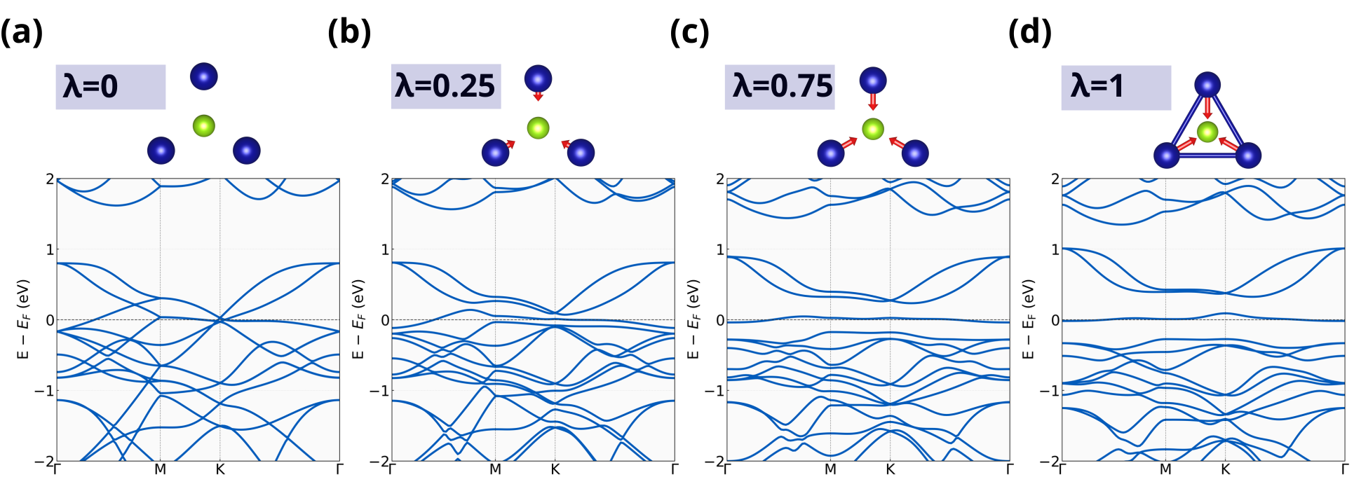
II.5 Polar distortion and flat-band emergence
To further clarify the microscopic origin of the flat band at the Fermi level, we investigated how the electronic structure evolves as the crystal is continuously distorted from the high-symmetry 11 phase toward the fully relaxed polar CDW state. Starting from the undistorted reference geometry, we generated a family of intermediate structures by linearly interpolating the atomic coordinates between the two endpoints. This procedure preserves the symmetry-breaking pattern characteristic of the CDW while allowing us to track, in a controlled fashion, the emergence of lattice polarization and trimer formation. Representative band structures along this interpolation coordinate are shown in Fig. 4.
At (undistorted phase, Fig. 4a), no flat band is present near the Fermi level. The manifold is relatively dispersive, and the spectral weight is spread over multiple bands without producing the strong real-space localization required for a flat band. As increases, the structural distortions associated with the CDW become appreciable: Cr trimers begin to form, and the out-of-plane polar displacement—absent in the high-symmetry structure—develops steadily (see Fig. 4b for ). The predominantly band begins to lose dispersion, indicating the onset of trimer molecular-orbital formation which is almost complete for (see Fig. 4c).
Upon approaching the fully relaxed CDW geometry (, Fig. 4d), the bonding–antibonding splitting within each trimer reaches its full magnitude. The antibonding -dominated state is driven upward in energy and ultimately becomes the flat, nearly dispersionless band pinned at the Fermi level.
This analysis demonstrates that lattice polarization and the associated inversion-symmetry breaking are essential ingredients for stabilizing the flat band. The gradual formation of trimer molecular orbitals reduces the effective hopping amplitudes within the Cr network, suppressing dispersion and driving the localization of the state. The flat band thus emerges from a structurally driven reorganization of the electronic degrees of freedom—one that cannot be achieved in the high-symmetry phase, even when spin polarization or spin–orbit coupling are included.

In order to illustrate how this flat band and the rise of strong correlations in this material can be controlled externally, we have carried out additional calculations introducing an electric field across the monolayer as sketched in Fig. 5a. This has been imposed as a saw-tooth potential that retains periodic boundary conditions, starting from a positive value at z=0, decreasing linearly until z=0.5 and then increasing linearly again towards z=1.0 (same as in z=0). By placing the monolayer centered at z= 0.25 or z= 0.75 (away from the abrupt change in the electric potential at z= 0.5), one can simulate a constant electric field. We have carried out two types of calculations. First, we fully relaxed the system from the NS configuration with an electric field. Eventually, the CDW phase in the phase emerges directly from the NS, in our case at about 70 MV/cm. In Fig. 5b we show the difference in Cr-Cr nearest neighbour distance, these are all equal in the NS, but there appears a short/long trimerization as the CDW emerges. This indicates that sufficiently large electric fields are capable of driving the system towards the polar phase, providing an external knob to create a strongly correlated state from a normal metallic one.
Additionally, we have carried out calculations in the polar CDW phase (the flat-band phase) at various electric fields. We observe that one can also control slightly the shape of the flat band itself. For example, we show in Figs. 5c and 5e that a pocket at appears at sufficiently large fields (compared to the flat band with no field in Fig. 5c), allowing for an additional degree of control of the shape of the flat band by an external electric field. Negative fields in our convention (opposing the polarization vector, like the bands shown in Fig. 5d) do not destroy the CDW once it has been stabilized. Instead, they drive the structure closer to the non-polar state while preserving the CDW distortion.
III Conclusions and Outlook
In this work, we have studied the structural, electronic, and magnetic properties of monolayer CrSe2 in its charge-density-wave (CDW) phase using density-functional theory. We demonstrate that this phase hosts a robust and nearly dispersionless flat band pinned at the Fermi level, which appears exclusively in the ferromagnetic CDW ground state and is absent in the high-symmetry 1T structure. Our results establish CrSe2 as a rare transition-metal dichalcogenide in which lattice distortions, orbital symmetry, and magnetism cooperate to produce flat-band physics.
The reconstruction leads to trimerization of Cr atoms within trigonally distorted CrSe6 octahedra and induces a pronounced polar displacement of the central Se atom, breaking inversion symmetry. As the trimer distortion and polar displacement develop, the -derived band progressively loses dispersion, ultimately forming a flat antibonding molecular state at the Fermi level. The magnetoelectric origin of the flat band paves the way for its possible control and tunability using external fields as knobs for controlling correlations in a 2D system via a mechanism that is fundamentally distinct from those in moiré systems or kagome lattices and not realized in related dichalcogenides with similar distortions. In particular, we show how an electric field can drive the system towards the polar phase, providing a way to control electronic correlations in the system. CrSe2 thus establishes a new paradigm for intrinsically generating flat bands through CDW-induced trimerization combined with polar distortions and magnetism. This cooperative mechanism suggests a promising route for engineering flat-band and correlated phases in low-dimensional materials without external patterning.
IV Computational Methods
All calculations were performed within the framework of density functional theory (DFT) Hohenberg and Kohn (1964); Kohn and Sham (1965) using the all-electron full-potential linearized augmented plane-wave (FP-LAPW) method as implemented in the WIEN2k code Blaha et al. (2020). The exchange–correlation energy was treated within the generalized gradient approximation (GGA), employing the Perdew–Burke–Ernzerhof (PBE) functional Perdew et al. (1996). On-site Coulomb interactions were introduced using the rotationally invariant LDA+ approach Petukhov et al. (2003), with Hubbard values varying from 0 to 5 eV in order to assess correlation effects on the electronic and magnetic properties.
Structural relaxations were performed at the GGA level using the VASP package Kresse and Furthmüller (1996a, b), allowing full optimization of internal coordinates and the in-plane lattice parameter. The plane-wave energy cutoffs ENCUT and ENAUG were set to 300 eV and 550 eV, respectively. For the FP-LAPW calculations, the parameter was set to 7.0, and muffin-tin radii of 2.37 and 2.10 a.u. were used for Cr and Se atoms, respectively. Brillouin-zone integrations were performed using a 12121 -point mesh.
Spin–orbit coupling (SOC) was included self-consistently using the second-variational procedure, with scalar-relativistic eigenfunctions as the basis. To model the isolated monolayer, a vacuum spacing of 15 Å was applied along the out-of-plane direction, eliminating spurious interlayer interactions. Both ferromagnetic and antiferromagnetic configurations were examined, including non-collinear arrangements within the supercell, and their relative energies were monitored as a function of to determine the magnetic ground state.
Electronic band structures and densities of states were obtained from the converged charge densities. Unfolded band structures, mapped onto the primitive Brillouin zone, were generated to enable a direct comparison between the distorted CDW phases and the parent 1T structure using Fold2BlochRubel et al. (2014); Wang et al. (1998).
acknowledgments
VP acknowledges support from the Ministry of Science of Spain through the Projects No. PID2021-122609NB-C22 and PID2024-161503NB-C22. SBC acknowledges support from the Ministry of Science of Spain through the Projects No. PID2021-122609NB-C21 and PID2024-161503NB-C21. We thank the CESGA (Centro de Supercomputacion de Galicia) for the computing facilities provided. J.C.S. thanks the support of the Ministry of Science and Education through the FPU Program (FPU22/01312). A.O.F. acknowledges support from the Academy of Finland Project No. 369367. Xunta de Galicia is acknowledged for projects ED431F 2022/005 and ED431B 2023/055.
References
- Novoselov et al. (2016) K S Novoselov, Artem Mishchenko, Alexandra Carvalho, and AH Castro Neto, “2D materials and van der Waals heterostructures,” Science 353, aac9439 (2016).
- Aoki (2020) Hideo Aoki, “Theoretical possibilities for flat band superconductivity,” Journal of Superconductivity and Novel Magnetism 33, 2341–2346 (2020).
- Iglovikov et al. (2014) VI Iglovikov, F Hébert, B Grémaud, GG Batrouni, and RT Scalettar, “Superconducting transitions in flat-band systems,” Physical Review B 90, 094506 (2014).
- Chan et al. (2022) Si Min Chan, Benoît Grémaud, and GG Batrouni, “Designer flat bands: Topology and enhancement of superconductivity,” Physical Review B 106, 104514 (2022).
- Tasaki (1998) Hal Tasaki, “From nagaoka’s ferromagnetism to flat-band ferromagnetism and beyond: An introduction to ferromagnetism in the Hubbard model,” Progress of theoretical physics 99, 489–548 (1998).
- Checkelsky et al. (2024) Joseph G Checkelsky, B Andrei Bernevig, Piers Coleman, Qimiao Si, and Silke Paschen, “Flat bands, strange metals and the Kondo effect,” Nature Reviews Materials 9, 509–526 (2024).
- Neupert et al. (2022) Titus Neupert, M Michael Denner, Jia-Xin Yin, Ronny Thomale, and M Zahid Hasan, “Charge order and superconductivity in kagome materials,” Nature Physics 18, 137–143 (2022).
- Teng et al. (2022) Xiaokun Teng, Lebing Chen, Feng Ye, Elliott Rosenberg, Zhaoyu Liu, Jia-Xin Yin, Yu-Xiao Jiang, Ji Seop Oh, M Zahid Hasan, Kelly J Neubauer, et al., “Discovery of charge density wave in a kagome lattice antiferromagnet,” Nature 609, 490–495 (2022).
- Chen et al. (2024) Y Chen, J Gaudet, GG Marcus, T Nomoto, T Chen, T Tomita, M Ikhlas, HS Suzuki, Yang Zhao, WC Chen, et al., “Intertwined charge and spin density waves in a topological kagome material,” Physical Review Research 6, L032016 (2024).
- Wilson and Ortiz (2024) Stephen D Wilson and Brenden R Ortiz, “A V3Sb5 kagome superconductors,” Nature Reviews Materials 9, 420–432 (2024).
- Cao et al. (2018a) Yuan Cao, Valla Fatemi, Ahmet Demir, Shiang Fang, Spencer L Tomarken, Jason Y Luo, Javier D Sanchez-Yamagishi, Kenji Watanabe, Takashi Taniguchi, Efthimios Kaxiras, et al., “Correlated insulator behaviour at half-filling in magic-angle graphene superlattices,” Nature 556, 80–84 (2018a).
- Cao et al. (2018b) Yuan Cao, Valla Fatemi, Shiang Fang, Kenji Watanabe, Takashi Taniguchi, Efthimios Kaxiras, and Pablo Jarillo-Herrero, “Unconventional superconductivity in magic-angle graphene superlattices,” Nature 556, 43–50 (2018b).
- Phillips et al. (2024) Jan Phillips, Jose L Lado, Victor Pardo, and Adolfo O Fumega, “Self-doped flat band and spin-triplet superconductivity in monolayer 1T-TaSe2-xTex,” Journal of Physics: Condensed Matter 36, 385804 (2024).
- Bianco et al. (2020) Raffaello Bianco, Lorenzo Monacelli, Matteo Calandra, Francesco Mauri, and Ion Errea, “Weak dimensionality dependence and dominant role of ionic fluctuations in the charge-density-wave transition of NbSe2,” Physical Review Letters 125, 106101 (2020).
- Neto (2001) AH Castro Neto, “Charge density wave, superconductivity, and anomalous metallic behavior in 2D transition metal dichalcogenides,” Physical review letters 86, 4382 (2001).
- Vaňo et al. (2021) Viliam Vaňo, Mohammad Amini, Somesh C Ganguli, Guangze Chen, Jose L Lado, Shawulienu Kezilebieke, and Peter Liljeroth, “Artificial heavy fermions in a van der Waals heterostructure,” Nature 599, 582–586 (2021).
- Crippa et al. (2024) Lorenzo Crippa, Hyeonhu Bae, Paul Wunderlich, Igor I Mazin, Binghai Yan, Giorgio Sangiovanni, Tim Wehling, and Roser Valentí, “Heavy fermions vs doped mott physics in heterogeneous Ta-dichalcogenide bilayers,” Nature communications 15, 1357 (2024).
- Dalal et al. (2025) Amir Dalal, Jonathan Ruhman, and Jörn WF Venderbos, “Flat band physics in the charge-density wave state of 1T-TaS2 and 1T-TaSe2,” npj Quantum Materials 10, 31 (2025).
- Wan et al. (2023a) Wen Wan, Rishav Harsh, Antonella Meninno, Paul Dreher, Sandra Sajan, Haojie Guo, Ion Errea, Fernando de Juan, and Miguel M Ugeda, “Evidence for ground state coherence in a two-dimensional Kondo lattice,” Nature communications 14, 7005 (2023a).
- Sugawara et al. (2016) Katsuaki Sugawara, Yuki Nakata, Ryota Shimizu, Patrick Han, Taro Hitosugi, Takafumi Sato, and Takashi Takahashi, “Unconventional charge-density-wave transition in monolayer 1T-TiSe2,” ACS nano 10, 1341–1345 (2016).
- Sipos et al. (2008) Balazs Sipos, Anna F Kusmartseva, Ana Akrap, Helmut Berger, Laszlo Forró, and Eduard Tutiš, “From mott state to superconductivity in 1T-TaS2,” Nature materials 7, 960–965 (2008).
- Liu et al. (2013) Y Liu, R Ang, WJ Lu, 1WH Song, LJ Li, and YP Sun, “Superconductivity induced by se-doping in layered charge-density-wave system 1T-TaS2-xSex,” Applied Physics Letters 102 (2013).
- Ramachandran et al. (2017) Ajith Ramachandran, Alexei Andreanov, and Sergej Flach, “Chiral flat bands: Existence, engineering, and stability,” Physical Review B 96, 161104 (2017).
- Bae et al. (2023) Jun-Hyung Bae, Tigran Sedrakyan, and Saurabh Maiti, “Isolated flat bands in 2D lattices based on a novel path-exchange symmetry,” SciPost Physics 15, 139 (2023).
- Hase et al. (2018) I Hase, T Yanagisawa, and K Kawashima, “Computational design of flat-band material,” Nanoscale research letters 13, 63 (2018).
- Zhang et al. (2020) Zhiming Zhang, Yimeng Wang, Kenji Watanabe, Takashi Taniguchi, Keiji Ueno, Emanuel Tutuc, and Brian J LeRoy, “Flat bands in twisted bilayer transition metal dichalcogenides,” Nature Physics 16, 1093–1096 (2020).
- Wan et al. (2023b) Xiaohan Wan, Siddhartha Sarkar, Shi-Zeng Lin, and Kai Sun, “Topological exact flat bands in two-dimensional materials under periodic strain,” Physical review letters 130, 216401 (2023b).
- Park et al. (2020) Youngju Park, Bheema Lingam Chittari, and Jeil Jung, “Gate-tunable topological flat bands in twisted monolayer-bilayer graphene,” Physical Review B 102, 035411 (2020).
- Gruner (2018) George Gruner, Density waves in solids (CRC press, 2018).
- Johannes and Mazin (2008) MD Johannes and II Mazin, “Fermi surface nesting and the origin of charge density waves in metals,” Physical Review B—Condensed Matter and Materials Physics 77, 165135 (2008).
- Balseiro and Falicov (1979) CA Balseiro and LM Falicov, “Superconductivity and charge-density waves,” Physical Review B 20, 4457 (1979).
- Lian et al. (2018) Chao-Sheng Lian, Chen Si, and Wenhui Duan, “Unveiling charge-density wave, superconductivity, and their competitive nature in two-dimensional NbSe2,” Nano letters 18, 2924–2929 (2018).
- Fumega et al. (2019) Adolfo O Fumega, Marco Gobbi, Paul Dreher, Wen Wan, Carmen González-Orellana, Marina Peña-Díaz, Celia Rogero, Javier Herrero-Martin, Pierluigi Gargiani, Max Ilyn, et al., “Absence of ferromagnetism in VSe2 caused by its charge density wave phase,” The Journal of Physical Chemistry C 123, 27802–27810 (2019).
- Lian et al. (2019) Chao Lian, Zulfikhar A Ali, and Bryan M Wong, “Charge density wave hampers exciton condensation in 1T-TiSe2,” Physical Review B 100, 205423 (2019).
- Rossnagel (2011) K Rossnagel, “On the origin of charge-density waves in select layered transition-metal dichalcogenides,” Journal of Physics: Condensed Matter 23, 213001 (2011).
- Yuan et al. (2019) Shuoguo Yuan, Xin Luo, Hung Lit Chan, Chengcheng Xiao, Yawei Dai, Maohai Xie, and Jianhua Hao, “Room-temperature ferroelectricity in MoTe2 down to the atomic monolayer limit,” Nature communications 10, 1775 (2019).
- Phillips et al. (2025) Jan Phillips, Adolfo O. Fumega, S. Blanco-Canosa, and Victor Pardo, “Ab initio description of the family of Cr selenides: Structure, magnetism, and electronic structure from bulk to the single-layer limit,” Phys. Rev. B 112, 224105 (2025).
- Liu et al. (2022) Yuhang Liu, Sohee Kwon, George J de Coster, Roger K Lake, and Mahesh R Neupane, “Structural, electronic, and magnetic properties of CrTe2,” Physical Review Materials 6, 084004 (2022).
- Li et al. (2021) Bo Li, Zhong Wan, Cong Wang, Peng Chen, Bevin Huang, Xing Cheng, Qi Qian, Jia Li, Zhengwei Zhang, Guangzhuang Sun, et al., “Van der waals epitaxial growth of air-stable CrSe2 nanosheets with thickness-tunable magnetic order,” Nature materials 20, 818–825 (2021).
- Cui et al. (2024) Fangfang Cui, Kun He, Shengqiang Wu, Hongmei Zhang, Yue Lu, Zhenzhu Li, Jingyi Hu, Shuangyuan Pan, Lijie Zhu, Yahuan Huan, et al., “Stoichiometry-tunable synthesis and magnetic property exploration of two-dimensional chromium selenides,” ACS nano 18, 6276–6285 (2024).
- Freitas et al. (2015) Daniele C Freitas, Ruben Weht, André Sulpice, Gyorgy Remenyi, Pierre Strobel, Frédéric Gay, Jacques Marcus, and Manuel Núnez-Regueiro, “Ferromagnetism in layered metastable 1T-CrTe2,” Journal of Physics: Condensed Matter 27, 176002 (2015).
- Zhang et al. (2021) Xiaoqian Zhang, Qiangsheng Lu, Wenqing Liu, Wei Niu, Jiabao Sun, Jacob Cook, Mitchel Vaninger, Paul F Miceli, David J Singh, Shang-Wei Lian, et al., “Room-temperature intrinsic ferromagnetism in epitaxial CrTe2 ultrathin films,” Nature communications 12, 2492 (2021).
- Lv et al. (2015) HY Lv, WJ Lu, DF Shao, Y Liu, and YP Sun, “Strain-controlled switch between ferromagnetism and antiferromagnetism in 1T-CrX2 (X= Se, Te) monolayers,” Physical Review B 92, 214419 (2015).
- Freitas et al. (2013) Daniele C Freitas, Matias Nunez, Pierre Strobel, André Sulpice, Ruben Weht, Armando A Aligia, and Manuel Nunez-Regueiro, “Antiferromagnetism and ferromagnetism in layered 1T-CrSe2 with V and Ti replacements,” Physical Review B—Condensed Matter and Materials Physics 87, 014420 (2013).
- Otero Fumega et al. (2020) Adolfo Otero Fumega, Jan Phillips, and Victor Pardo, “Controlled two-dimensional ferromagnetism in 1T-CrTe2: the role of charge density wave and strain,” The Journal of Physical Chemistry C 124, 21047–21053 (2020).
- Jindal et al. (2023) Apoorv Jindal, Amartyajyoti Saha, Zizhong Li, Takashi Taniguchi, Kenji Watanabe, James C Hone, Turan Birol, Rafael M Fernandes, Cory R Dean, Abhay N Pasupathy, et al., “Coupled ferroelectricity and superconductivity in bilayer Td-MoTe2,” Nature 613, 48–52 (2023).
- Hou et al. (2019) Wenhui Hou, Ahmad Azizimanesh, Arfan Sewaket, Tara Peña, Carla Watson, Ming Liu, Hesam Askari, and Stephen M Wu, “Strain-based room-temperature non-volatile MoTe2 ferroelectric phase change transistor,” Nature nanotechnology 14, 668–673 (2019).
- Wang et al. (2020) YD Wang, WL Yao, ZM Xin, TT Han, ZG Wang, L Chen, C Cai, Yuan Li, and Y Zhang, “Band insulator to Mott insulator transition in 1T-TaS2,” Nature communications 11, 4215 (2020).
- Hohenberg and Kohn (1964) Pierre Hohenberg and Walter Kohn, “Inhomogeneous electron gas,” Physical review 136, B864 (1964).
- Kohn and Sham (1965) Walter Kohn and Lu Jeu Sham, “Self-consistent equations including exchange and correlation effects,” Physical review 140, A1133 (1965).
- Blaha et al. (2020) Peter Blaha, Karlheinz Schwarz, Fabien Tran, Robert Laskowski, Georg KH Madsen, and Laurence D Marks, “WIEN2K: An APW+ lo program for calculating the properties of solids,” The Journal of chemical physics 152 (2020).
- Perdew et al. (1996) John P Perdew, Kieron Burke, and Matthias Ernzerhof, “Generalized gradient approximation made simple,” Physical review letters 77, 3865 (1996).
- Petukhov et al. (2003) AG Petukhov, II Mazin, Liviu Chioncel, and AI Lichtenstein, “Correlated metals and the LDA+U method,” Physical Review B 67, 153106 (2003).
- Kresse and Furthmüller (1996a) Georg Kresse and Jürgen Furthmüller, “Efficient iterative schemes for ab initio total-energy calculations using a plane-wave basis set,” Physical review B 54, 11169 (1996a).
- Kresse and Furthmüller (1996b) Georg Kresse and Jürgen Furthmüller, “Efficiency of ab-initio total energy calculations for metals and semiconductors using a plane-wave basis set,” Computational materials science 6, 15–50 (1996b).
- Rubel et al. (2014) O Rubel, A Bokhanchuk, SJ Ahmed, and E Assmann, “Unfolding the band structure of disordered solids: From bound states to high-mobility Kane fermions,” arXiv preprint arXiv:1405.4218 (2014).
- Wang et al. (1998) L-W Wang, L Bellaiche, S-H Wei, and A Zunger, “Majority representation of alloy electronic states,” Physical review letters 80, 4725 (1998).