A High Efficiency Superconducting On-chip Filterbank with Directional Filters for Integral Field Units in the Sub-millimeter Regime
Abstract
Integrated superconducting spectrometers are developing to the point that they are enabling integral field units, providing large area spectral mapping capabilities for astronomy in the sub-millimeter band. However, these integral field units are only worthwhile if they have a high efficiency, but to date the efficiency of on-chip filterbanks has been quite poor. Here we demonstrate a filterbank with high efficiency by using directional filters. Using a cryogenic thermal load and a noise measurement in combination with a continuous-wave terahertz source to obtain the spectral response of the filters, we are able to accurately measure the filterbank efficiency, accounting for all quasi-optical elements within our setup. We experimentally obtain an average peak coupling efficiency to the detectors of 75% in a filterbank that sparsely samples between 125 GHz to 220 GHz using filters with a mean loaded quality factor of 19.6. Our results demonstrate that a filterbank with a high efficiency is achievable using directional filters, giving a clear route towards efficient integral field units.
I Introduction
The integrated superconducting spectrometer (ISS) [35, 31, 32, 1, 25] is maturing to the point that integral field units (IFUs) with ISSs are becoming feasible at (sub-)millimeter wavelengths [18, 10, 1, 21]. These IFUs will provide a large field-of-view and a broad spectral bandwidth with moderate spectral resolution, enabling several observing techniques such as (sub-)millimeter-wave line-intensity mapping [33, 20, 23, 15], unbiased surveys of dusty line-emitting galaxies [39, 22], galaxy-cluster analysis using the Sunyaev-Zeldovich effect [9, 27], and spectro-polarimetry of the CMB [7, 34]. Thanks to the integration on a wafer, ISS-based IFUs are far more compact and scalable compared to their quasi-optical analogs (e.g. FTS [36, 17, 8], FPI [5], grating [13, 2]), and do not require any opto-mechanics. Hence, the ISS-based IFUs are regarded as the enabling technology for large-format 3D surveyors on existing telescope facilities (e.g. ASTE, APEX, SPT [42]), and on future large telescopes, like CCAT/FYST [28] or the proposed 50m AtLAST telescope [26].
The IFU is an array of spaxels (spatial pixels), each of which is an independent ISS consisting of a lens-antenna, a superconducting on-chip filterbank with tens to hundreds of spectral channels, and a kinetic inductance detector (KID) at the output of each filter. The array of KIDs is read out making use of frequency multiplexing, allowing 1000 KIDs per readout line [40]. The compactness of the filterbanks and the simple multiplexing of KIDs is exactly what enables the scaling of IFUs toward larger arrays.
However, upscaling to a large IFU would only be worthwhile if the individual ISS spaxels have a high sensitivity. To achieve a high sensitivity, each ISS spaxel must be 1) photon-noise limited, i.e., no instrumental noise in addition to the intrinsic thermal noise of the photons from the foreground atmosphere, and 2) have a high coupling efficiency from the lens to the KIDs. The ISS technology has proven photon-noise limited operation on a ground-based telescope [12], but the efficiency has been low, limiting the total sensitivity, and therefore the surveying speed, of the system.
Existing on-chip spectrometers lose more than \qty75 of the incoming signal at the peak coupling efficiency of individual channels. This is due to dielectric losses in the filterbank [3], overlapping sidebands from the filters, and due to the fundamental \qty50 coupling limitation for half-wave resonator filters [24], which are typically used in on-chip filterbanks [31, 35, 32]. The current highest measured efficiency of a densely sampled on-chip filterbank is an average of \qty16 peak coupling efficiency with a Q-factor of 340 across 334 channels [19], or \qty27 peak efficiency when arrayed in a spectrally sparse configuration [29]. The maximum coupling efficiency can ideally be improved to \qty100 by using a coherent filter architecture such as a directional filter, instead of a half-wave resonator structure [24].
Here we experimentally demonstrate the high coupling efficiency of directional filters. We fabricated a filterbank with a spectral coverage from 125 GHz to 220 GHz and a loaded quality factor of 25. We place the filters in our filterbank such that they sparsely fill the frequency space, giving a total of eight channels with very limited overlap in the filter bands, allowing us to study the filter behavior in detail without the added complexity of filter overlap. The design and fabrication of our device are discussed in Section II and Section III, respectively. The efficiency of the filterbank was measured using a combination of a cryogenic blackbody measurement and a continuous-wave terahertz source. The methods for our measurement and analysis are described in Section IV and the results are discussed in Section V.
II Device Design

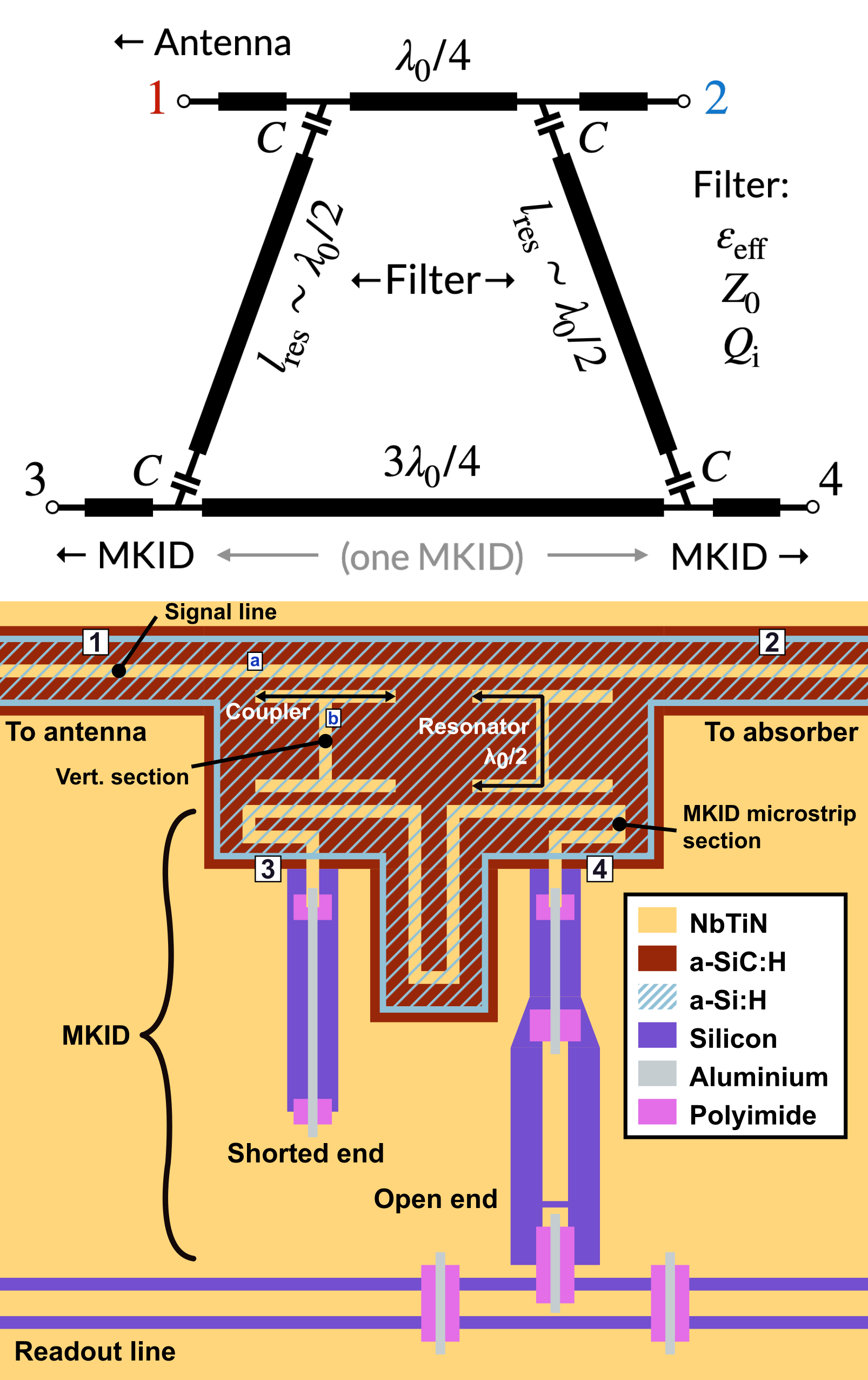

The device is shown in Figure 1a. The chip and holder are based very closely on the DESHIMA 1.0 design [12, 11] (twinslot antenna, lens and holder), with a sparse filterbank using a microstrip based filter design using fabrication technology similar to DESHIMA 2.0 [35, 19]. In this work we realize a sparse configuration of a filterbank that is designed to cover a bandwidth of one octave from 135 GHz to 270 GHz with a filter spacing equal to a spectral resolution R of 30 and a loaded quality factor of 25, which makes the filterbank design slightly oversampled. The number of filters for this spectral resolution is given by
| (1) |
where is the ceiling function, and results in 22 filters in the band. Each resonator has a resonance given by
| (2) |
We use a sparse filterbank configuration to be able to study the individual filter responses without being affected by the overlapping sidebands of neighboring filters [24]. This is realized by only patterning one in every three filters, which can be seen in the microscope image in Figure 1e.

II-A Filter design
The filterbank consists of directional filters [24]. A circuit model and a schematic of the directional filter as implemented in our device is given in Figure 2. The directional filter creates an impedance matched condition on- and off-resonance by using a phase-coherent structure. This leads to a more efficient coupling to the KID, overcoming the \qty50 maximum peak coupling efficiency of half-wave filters.
The filters are designed with a loaded quality factor of 25 to minimize the influence of dielectric losses on our experiment [29, 3]. The coupling strength across a single coupling element and the coupling quality factor are related with
| (3) |
and the loaded quality factor of a resonator surrounded by two of these couplers is given by
| (4) |
where represents the internal losses of the resonator. For our dielectric materials, detailed in Section III, we expect a between . Since , the internal losses can be neglected and, by combining Equation 3 and Equation 4, it can be found that for a loaded quality factor of 25 a coupling strength is required.
To reach this required coupling strength, we adapt the DESHIMA 2.0 design [19] by adding a top dielectric on the microstrip co-planar coupler. A schematic drawing of the coupler in the filter is shown in Figure 2 with micrographs of the realized coupler in Figure 1c-d. We find that we need a gap of \qty250\nano and an a-Si capping layer of \qty800\nano to reach using SONNET simulations, as shown in Figure 3.
Furthermore, this simulation is used to find the exact coupling bar length to reach the desired coupling strength at each individual filter resonance frequency. Note that the resonators in the filterbank have an electrical length of , where is the wavelength. This constraint requires that the coupling bar length should be less than . Since we are near the peak coupling strength of this coupler design, it is only slightly shorter than , indicating that we are at the lower limit of for our current coupling geometry.
Using the material parameters of the NbTiN, a-SiC:H, and a-Si:H (see Section III), we define the filter geometry and electrical properties in Table I.
| width (\unit\micro) | (\unitΩ) | ||
|---|---|---|---|
| Signal line | |||
| Coupler | |||
| Vertical section | |||
| KID microstrip section |
We implemented this filterbank into a transmission line model to predict the frequency response of our device [24, 29]. We used the measured layer thicknesses and widths that were obtained using the micrographs in Figure 1, and we used the measured material parameters specified in Section III. The sparse, low spectral resolution filterbank configuration results in an average simulated peak efficiency of \qty80 as shown in Figure 4. This is a \qty20 deviation from a \qty100 percent peak coupling efficiency for a perfect system [24]. This is because at strong coupling, the coupler cannot be approximated by a perfect admittance inverter [30], causing a small reflection on the signal line at resonance. Decreasing the admittance of the resonator mitigates this problem slightly, but was not implemented for this device as this would have made the width of the coupling elements too narrow for fabrication. Furthermore, the residual overlapping sidebands of the filters slightly reduces the peak coupling efficiency due to leakage to these preceding filters.
II-B KID design
The quarter-wave KIDs in our filterbank are illustrated in Figure 2 and have a unique geometry because they also form the impedance match with the directional filter at sub-millimeter frequencies, which is required for its proper operation. The lossy aluminium-NbTiN (hybrid) CPW lines absorb the sub-millimeter signal and form an input impedance approximately equal to the characteristic impedance of the hybrid lines, as long as the total attenuation is significant [30], i.e. the reflectance amplitude as seen at the ports is sufficiently small.
We have a hybrid CPW line with a complex propagation constant which gives an attenuation of \qty14\per at \qty190. Its length is \qty1 and is divided between port 3 and 4. We favour a longer length at port 3, since almost all power from the antenna couples to this port, and we ensure there is sufficient length left at port 4 to reasonably approximate this input inpedance with its characteristic impedance. Furthermore, we couple port 3 of the filter to the shorted end of the KID to maximize the response by absorbing the signal at its current maximum. It should also be noted that the NbTiN microstrip section that is part of the filter separates the quasiparticle systems of the two sections of aluminium. As a consequence of this, the volume of the aluminium at the shorted end is the effective aluminium volume of the KID. We find that a 2/3 to 1/3 split for ports 3 and 4, respectively, are optimum. This gives an input reflectance amplitude at ports 3 and 4 that is attenuated with \qty9.5 and \qty4.7, respectively.
Finally, we give the design parameters of the KIDs. There are eight filter KIDs designed between \qty5.4 and \qty6.6 with a equal to . There are four wideband KIDs designed around \qty6.75 with \qty30\mega spacing and a equal to . The sub-millimeter signal is weakly wideband-coupled to two KIDs before the filterbank and two after the filterbank, which we will call ‘widebands before’ and ‘widebands after,’ respectively. Lastly, there are two blind KIDs at \qty5.25 and \qty5.3 with a equal to . One is near the start of the filterbank and one is near the end of the filterbank.
III Fabrication
The fabrication route of this chip is nearly identical to the one described in [16], for the filter fabrication, we closely mimic the process described in [37]. The only difference is the addition of an \qty800\nano a-Si:H layer on top of the filterbank deposited using PECVD at \qty250 and patterned using optical contact lithography and etched using an SF6 and O2 plasma in a reactive-ion etcher (RIE).
With the extra layer, the bottom-to-top stratification of the filterbank structure is: 200 nm NbTiN (, , ) [38], 500 nm a-SiC:H (, ) [3], 200 nm NbTiN, and, 800 nm a-Si:H (, ) [4, 29]. This stratification is also visible in the micrograph in Figure 1d. Note that we have two different dielectrics in the stratification, this is solely due to machine availability at the time of fabricating.
These four layers in the filterbank stratification are the first layers that are deposited, patterned and etched on the chip. The fabrication is completed with \qty1\micro thick Polyimide patches for the readout line bridges; 40 nm aluminium (, ) for the KIDs and the bridges; and, 40 nm of -phase tantalum (, ) on the backside for stray light control [41]. After fabrication, the chip is diced and the lens with a spacer wafer is glued to the backside of the wafer. The chip is finally mounted in the holder as shown in Figure 1a.
IV Methods
To measure the filterbank efficiency, the chip is placed into an adiabatic demagnetization refrigeration (ADR) cryostat cooled to 120 mK. Our setup is shown in Figure 5a. This setup is similar to the experiment described in [6] and allows us to illuminate the chip and lens with a cryogenic blackbody, capable of radiating with a temperature from 4 K to 40 K. The efficiency is found using a two step process.
Firstly, we experimentally obtain the coupling efficiency between the detectors and a well defined cryogenic thermal radiator using the photon noise as absolute calibration [14]. This is discussed in Section IV-A.
Secondly, we measure the frequency response of the filters using a continuous-wave (CW) terahertz source with uncalibrated power output, similar to [12]. This provides the relative frequency response of the filters which is normalized and is applied as the final element in the optical path. This is discussed in Section IV-B.

IV-A Optical efficiency
First, we define the frequency response of the filters from the reference plane in front of the filterbank as shown in Figure 5c, to the KID detector as follows
| (5) |
In this equation, is the frequency-independent unknown filter efficiency of filter which we aim to find and is the normalized frequency response which we will obtain from our CW terahertz source measurement, which is explained in Section IV-B.
The power absorbed in the aluminium of the KID behind filter is given by
| (6) |
Where is the blackbody specific intensity at a known temperature which is converted to a single polarization using the factor 1/2, is the is the free-space wavelength, and is the transfer efficiency from the blackbody to the reference plane. We use in Equation 6 to denote the power spectral density that can be absorbed in the KID for a filter efficiency with a peak value of unity.
The transfer efficiency is decomposed as follows
| (7) |
where the comprising terms are defined as:
-
–
The filterstack efficiency is the transmission of the filterstack used to limit the blackbody radiation to our band of interest. It has two configurations which are shown in Figure 5b.
-
–
The radiation efficiency is defined as the fraction of the power radiated over the power used to excite the antenna, accounted for the power reflected at the Si-vacuum lens interface. This is calculated using a quasi-optical simulation [43] for our twin-slot antenna with a hyper-hemispherical lens.
-
–
The forward efficiency defines what fraction of the total radiated power by the antenna is actually radiated in the upper plane of the antenna, in the direction of the lens and blackbody source. This is found from the simulated radiation patterns of the lens-antenna.
-
–
The matching efficiency defines how well the antenna impedance is matched to the line impedance of the on-chip CPW line, and is calculated with the Thevenin equivalent circuit shown in Figure 5c. Since a twin-slot antenna is resonant, it will have a designed peak matching efficiency at the center of the operation band, which for our antenna is designed to be at 220 GHz.
Note that the antenna observes the blackbody through an aperture, which would normally require an spillover efficiency. However, the lens-antenna beam is much narrower than the aperture diameter and of the beam sees the blackbody source, therefore the spillover efficiency is neglected.
We verified our calculations of the coupling efficiency to the reference plane by measuring the efficiency of the wideband KIDs in front of the filterbank using the narrow-band filterstack configuration as shown in Figure 5b.
The results are shown in Figure 6.
Across the narrow-band filterstack, the coupling strength of the wideband coupler can be considered constant, which means we do not need to make any assumptions for the frequency dependence of the wideband couplers.
Instead, we can directly compare the measured efficiency to the expected efficiency of the wideband-coupled KIDs.
The expected efficiency is obtained from a SONNET simulation using the measured geometry and material parameters.
We explicitly take into account an overetch of \qty100\nano into the a-SiC:H, wich is filled by a-Si:H, and the thickness of the metals.
The results show that we measure the expected coupling efficiency using our method, validating our calculations for .

Since we know we can experimentally obtain , using the method described by Ferrari et al. [14]. This method equates the experimentally measured noise equivalent power (), which is obtained via a noise measurement and a responsivity measurement, with the theoretical NEP given by the incident power as defined in Equation 6. The experimental NEP is
| (8) |
where is the phase noise at white photon noise level (i.e. at sampling frequencies below the quasiparticle lifetime rolloff). We find the white photon noise level of each KID by fitting the noise using a composite model to isolate it from the 1/f noise and readout noise, the details of our fitting procedure are described in the Appendix. The responsivity is the phase response due to a change in the incident power, which is measured by performing a sweep of the blackbody temperature of a few kelvin around .
Secondly, the theoretical photon noise limited NEP for a KID calculated from in Equation 6 is expressed as
| (9) |

IV-B Normalization of the filter frequency response
Using a CW terahertz source, we obtain the unnormalized relative frequency response as follows. The CW terahertz source illuminates the chip mounted in a second setup (see [11] for details) and the source is swept from \qtyrange90300\giga with steps of \qty50\mega. Each KID observes the phase response to this signal. There are a few wideband-coupled KIDs that are weakly coupled to the signal line from the antenna, which can be seen in Figure 5. These act as a power reference for the on-chip components. They are used to remove the power fluctuations of the CW terahertz source and other coherent external influences by dividing the responses of the filter KIDs with the average of the wideband-coupled KIDs before the filterbank. This results in the unnormalized relative frequency response at the reference plane. Furthermore, an estimate of the relative power transmitted across the filterbank can be calculated by dividing the response of the widebands after the filterbank by the response of the widebands before the filterbank.
To get a physically correct efficiency result and complete the optical efficiency calculation, this relative frequency response needs to be normalized to obtain as defined in Equation 5. Ideally, the normalization is simply applied by normalizing each filter with its maximum value, which satisfies the aforementioned condition. However, as we will observe in the measurements, a standing wave is present on the signal line of the filterbank. This distorts the filter response with a ripple, making the standard normalization unreliable.
Instead, we use a normalization based on the total area under each filter in combination with its known spectral shape in (semi-)isolation, to integrate out the distortions due to standing waves. Each filter in (semi-)isolation has a lorentzian filter shape. We define a standard lorentzian with a loaded quality factor , resonance frequency and a peak intensity as
| (11) |
The total area of the lorentzian is
| (12) |
and the integral across the full-width half maximum (FWHM) is exactly half the total area
| (13) |
The loaded Q-factor is calculated using the bandwidth at the FWHM.
Besides the lorentzian spectral shape assumption, we assume that the couplers have the same across the band, as designed. This implies that the area under the frequency-normalized response of all filters is equal. However, we must not neglect a possible systematic difference in due to the fabrication, making a constant, but unknown parameter of the lorentzian filter shape. We must therefore first determine before applying the normalization.
The normalization procedure is as follows. First, the data of each filter is expressed in terms of its normalized frequency . Then, each filter is normalized by its total area. This normalizes each filter with the same but unknown scaling factor , where the factor comes from the lorentzian integral. To find , the average of all the normalized filters is taken. From the average normalized response, its FWHM is found by making use of Equation 13, finding for what bandwidth the area around the resonance is half the total area. The is calculated from the FWHM. Finally, each individual normalized filter response is scaled with a factor to get the true normalized filter response, defined as in Equation 5. This gives us enough information for the efficiency calculations.
V Results & Discussion

The chip was mounted in its holder and measured. We found 12 out of 14 KIDs between 5 GHz to 7GHz, with 6 out of 8 filter KIDs, all four wideband KIDs and both blind KIDs found. We find an average KID of and an average of . We measured the noise of the KIDs in the setup of Figure 5 with the blackbody around a mean temperature of and we performed a blackbody sweep with a range of around the mean. The noise of all the KIDs is found to be significant, requiring a fit to extract the photon noise. The fitting procedure is described in the Appendix. One filter KID, KID 8, is found to have an abnormally high noise level due to spiking events, making a reliable estimate of the photon noise impossible. We will therefore exclude this KID from the efficiency calculation. For all the other KIDs we get a good fit on the noise, giving a reliable photon noise level to obtain the efficiency using Equation 10.
The raw wideband data, the filter responses with wideband reference, and the relative response of the wideband KIDs after the filterbank are shown in Figure 7. The dips in the power transmitted across the filterbank are quite deep and are approximately two orders of magnitude lower than the off-resonance baseline. These dips suggest that the filters are capturing or reflecting nearly all () the power. From the filterbank simulations in Figure 4 an on-resonance reflection of \qtyrange1020 is expected. To check this, we compare the amplitudes of the wideband couplers before the filterbank around \qty200, where their relative separation is . Here, the wideband amplitude envelope is proportional to for one of the wideband-coupled KIDs or for the other, which allows us to infer based on their relative amplitude difference. We find that the reflection varies between \qtyrange1045 around \qty200, which suggest that there is an additional reflectance above what we expect. These additional reflectances are also visible in the filter response in Figure 8a and we use the normalization method in Section IV-B to account for this.
Note that the two KIDs belonging to filters at 110 GHz and 135 GHz are missing, however their filter resonance dips are visible in the estimate of the power transmitted across the filterbank. So, that must mean the aluminium part of the KIDs must be connected to the filter structure, otherwise we should see large peaks in the wideband-coupled KIDs due to reflections.. This suggests that the filters still work as intended, despite having missing KIDs.
The relative filter responses are normalized according to Section IV-B, resulting in the normalized filter responses which are shown in Figure 8a. The normalized responses are stacked using a normalized frequency centered on the filter resonance. The average shape is approximately a lorentzian and the Q-factor is equal for all filters, validating our assumptions for our normalization method. The relatively strong ripple on the filter responses justifies the normalization method using an integrated lorentzian.
The noise and responsivity measurements are combined with the normalized filter frequency response measurement according to the methods in Section IV, resulting in an average measured efficiency of \qty75 as shown in Figure 8b. We find a , which is lower than the designed Q-factor and therefore the coupling strength is stronger than we simulated.
VI Conclusion
We designed, fabricated, and measured a sparsely sampled filterbank using directional filters. We measured a mean filter efficiency of \qty75, well in agreement with our model calculation, where the \qty25 reduction in coupling compared to a perfect isolated filter can be attributed to reflections at the filters. Besides this, we have also demonstrated a very low Q-factor of 19.6 for our on-chip filterbank using two parallel-coupled microstrip lines underneath a dielectric capping layer.
Our results show that coherent filters provide a very efficient filter solution for on-chip filterbank spectrometers, resulting in significantly higher coupling efficiency than conventional half-wave filters. The improvement in efficiency presented in this paper makes directional filters for on-chip spectrometers the most obvious choice for scaling toward large imaging spectrometers to be installed on current and future sub-millimeter telescope facilities.
Acknowledgment
Views and opinions expressed are those of the authors only and do not necessarily reflect those of the European Union or the European Research Council Executive Agency. Neither the European Union nor the granting authority can be held responsible for them.

Figure 9 is an example of a measured KID, showing the blackbody responsivity and a phase noise power spectral density measurement. For the responsivity to the blackbody, we take the average of the upsweep and downsweep phase responsivity in temperature. The hysteresis is due to the blackbody temperature lagging slightly with respect to the heater and the temperature sensor.
The noise is fit using a composite model with the following components:
-
1.
Photon noise with quasi-particle roll-off ()
-
2.
noise with resonator ring time roll-off ()
-
3.
noise with resonator ring time roll-off ()
-
4.
White readout noise
We initialize the fitting procedure by finding the flattest region between \qty1e1 and \qty1e4 using the minimum of the derivative of a smoothed phase noise function . The photon noise level minus 1 dB is the initial guess for the photon noise level. The initial value was set at a value slightly lower than the phase noise at 1 Hz. The initial value was set slightly lower than the value, to make it sub-dominant. During fitting, it became clear that independent and a terms are needed to fit the data well. A single term would not capture the slow to photon noise knee plus the slow photon noise roll-off to readout noise transistions simultaneously, therefore both were kept independent. This noise decomposition and fitting procedure proved very effective at finding the photon noise level for our KIDs, since they have a significant amount of noise.
References
- [1] (2025-10) Spectral characterization and performance of SPT-SLIM on-chip filterbank spectrometers. External Links: 2509.02245, Document Cited by: §I.
- [2] (2004-10) Z-Spec, a broadband millimeter-wave grating spectrometer–design, construction, and first cryogenic measurements. In Millimeter and Submillimeter Detectors for Astronomy II, Vol. 5498, pp. 257–267. External Links: Document Cited by: §I.
- [3] (2025-01) Vibrational modes as the origin of dielectric loss at 0.27–100 THz in a-SiC:H. Phys Rev Appl 23 (1), pp. 014035. External Links: ISSN 2331-7019, Document Cited by: §I, §II-A, §III.
- [4] (2022-06) Characterization of low-loss hydrogenated amorphous silicon films for superconducting resonators. J Astron Telesc Instrum Syst 8 (02). External Links: 2012.07692, ISSN 2329-4124, Document Cited by: §III.
- [5] (2020-05) The Design of the CCAT-prime Epoch of Reionization Spectrometer Instrument. J Low Temp Phys 199 (3), pp. 898–907. External Links: ISSN 1573-7357, Document Cited by: §I.
- [6] (2014-02) Fluctuations in the electron system of a superconductor exposed to a photon flux. Nat Commun 5 (1), pp. 3130. External Links: ISSN 2041-1723, Document Cited by: §IV.
- [7] (2019-09) Microwave Spectro-Polarimetry of Matter and Radiation across Space and Time. External Links: 1909.01591, Document Cited by: §I.
- [8] (2025-09) Continuum, CO, and water vapour maps of the Orion Nebula: First millimetre spectral imaging with CONCERTO. Astron Astrophys 701, pp. A210. External Links: ISSN 0004-6361, 1432-0746, Document Cited by: §I.
- [9] (2025-06) Atacama Large Aperture Submillimeter Telescope (AtLAST) science: Resolving the hot and ionized Universe through the Sunyaev-Zeldovich effect. Open Res Eur 4, pp. 113. External Links: ISSN 2732-5121, Document Cited by: §I.
- [10] (2025-10) An On-Sky Atmospheric Calibration of SPT-SLIM. External Links: 2510.14220, Document Cited by: §I.
- [11] (2019-06) Wideband on-chip terahertz spectrometer based on a superconducting filterbank. J Astron Telesc Instrum Syst 5 (3), pp. 035004. External Links: ISSN 2329-4124, 2329-4221, Document Cited by: §II, §IV-B.
- [12] (2019-11) First light demonstration of the integrated superconducting spectrometer. Nat Astron 3 (11), pp. 989–996. External Links: ISSN 2397-3366, Document Cited by: §I, §II, §IV.
- [13] (2012-09) Design and first-light performance of TES bolometer arrays for submillimeter spectroscopy with ZEUS-2. In Millimeter, Submillimeter, and Far-Infrared Detectors and Instrumentation for Astronomy VI, Vol. 8452, pp. 44–55. External Links: Document Cited by: §I.
- [14] (2018-01) Antenna Coupled MKID Performance Verification at 850 GHz for Large Format Astrophysics Arrays. IEEE Trans Terahertz Sci Technol 8 (1), pp. 127–139. External Links: ISSN 2156-3446, Document Cited by: §IV-A, §IV.
- [15] (2024-11) Forecasts and Statistical Insights for Line Intensity Mapping Cross-correlations: A Case Study with 21 cm × [C ii]. Astrophys J 975 (2), pp. 222. External Links: ISSN 0004-637X, Document Cited by: §I.
- [16] (2021-07) Superconducting Microstrip Losses at Microwave and Submillimeter Wavelengths. Phys Rev Appl 16 (1), pp. 014019. External Links: Document Cited by: §III.
- [17] (2024-09) CONCERTO at APEX On-sky performance in continuum. Astron Astrophys 689, pp. A20. External Links: ISSN 0004-6361, 1432-0746, Document Cited by: §I.
- [18] (2023-10) 2023 Astrophotonics Roadmap: pathways to realizing multi-functional integrated astrophotonic instruments. J Phys Photonics 5 (4), pp. 042501. External Links: ISSN 2515-7647, Document Cited by: §I.
- [19] (2026-01) DESHIMA 2.0: A 200-400 GHz Ultra-wideband Integrated Superconducting Spectrometer. External Links: 2601.21603, Document Cited by: §I, §II-A, §II.
- [20] (2024-11) [CII] line intensity mapping the epoch of reionization with the Prime-Cam on FYST - II. CO foreground masking based on an external catalog. Astron Astrophys 691, pp. A262. External Links: ISSN 0004-6361, 1432-0746, Document Cited by: §I.
- [21] (2020-12) Large format imaging spectrograph for the Large Submillimeter Telescope (LST). In Millimeter, Submillimeter, and Far-Infrared Detectors and Instrumentation for Astronomy X, pp. 24. External Links: 2102.08280, Document Cited by: §I.
- [22] (2025-12) Concept integral field unit spectrometer instrument for the next-generation millimeter-wave cosmological surveys. J Astron Telesc Instrum Syst 11 (4), pp. 045007. External Links: ISSN 2329-4124, 2329-4221, Document Cited by: §I.
- [23] (2025-08) Constraining the [C II] luminosity function from the power spectrum of line-intensity maps at redshift 3.6. Astron Astrophys 700, pp. A211. External Links: ISSN 0004-6361, 1432-0746, Document Cited by: §I.
- [24] (2024-05) Directional Filter Design and Simulation for Superconducting On-Chip Filter-Banks. J Low Temp Phys. External Links: ISSN 1573-7357, Document Cited by: §I, Figure 2, Figure 2, Figure 4, Figure 4, §II-A, §II-A, §II.
- [25] (2020-12) µ-spec spectrometers for the EXCLAIM instrument. In Millimeter, Submillimeter, and Far-Infrared Detectors and Instrumentation for Astronomy X, Vol. 11453, pp. 128–139. External Links: Document Cited by: §I.
- [26] (2025-02) The conceptual design of the 50-meter Atacama Large Aperture Submillimeter Telescope (AtLAST). Astron Astrophys 694, pp. A142. External Links: ISSN 0004-6361, 1432-0746, Document Cited by: §I.
- [27] (2019-02) Astrophysics with the Spatially and Spectrally Resolved Sunyaev-Zeldovich Effects. Space Sci Rev 215 (1), pp. 17. External Links: ISSN 1572-9672, Document Cited by: §I.
- [28] (2022-08) CCAT-prime: the Fred Young Submillimeter Telescope (FYST) final design and fabrication. In Ground-Based and Airborne Telescopes IX, Vol. 12182, pp. 543–550. External Links: Document Cited by: §I.
- [29] (2021-11) Terahertz Band-Pass Filters for Wideband Superconducting On-Chip Filter-Bank Spectrometers. IEEE Trans Terahertz Sci Technol 11 (6), pp. 635–646. External Links: ISSN 2156-3446, Document Cited by: §I, Figure 4, Figure 4, §II-A, §II-A, §III.
- [30] (2012) Microwave engineering. 4th ed edition, Wiley, Hoboken, NJ. External Links: ISBN 978-0-470-63155-3, LCCN TK7876 .P69 2012 Cited by: §II-A, §II-B.
- [31] (2022-11) SuperSpec: On-Chip Spectrometer Design, Characterization, and Performance. J Low Temp Phys 209 (3), pp. 548–555. External Links: ISSN 1573-7357, Document Cited by: §I, §I.
- [32] (2022-11) The Simulation and Design of an On-Chip Superconducting Millimetre Filter-Bank Spectrometer. J Low Temp Phys 209 (3-4), pp. 493–501. External Links: ISSN 0022-2291, 1573-7357, Document Cited by: §I, §I.
- [33] (2024-06) Cross-correlation Techniques to Mitigate the Interloper Contamination for Line Intensity Mapping Experiments. Astrophys J 969 (1), pp. 2. External Links: ISSN 0004-637X, Document Cited by: §I.
- [34] (2013-09) Detection of B-Mode Polarization in the Cosmic Microwave Background with Data from the South Pole Telescope. Phys Rev Lett 111 (14), pp. 141301. External Links: Document Cited by: §I.
- [35] (2022-11) DESHIMA 2.0: Development of an Integrated Superconducting Spectrometer for Science-Grade Astronomical Observations. J Low Temp Phys 209 (3), pp. 278–286. External Links: ISSN 1573-7357, Document Cited by: §I, §I, §II.
- [36] (2020-10) A wide field-of-view low-resolution spectrometer at APEX: Instrument design and scientific forecast. Astron Astrophys 642, pp. A60. External Links: ISSN 0004-6361, 1432-0746, Document Cited by: §I.
- [37] (2022-09) Combined ultraviolet- and electron-beam lithography with Micro-Resist-Technology GmbH ma-N1400 resist. J Vac Sci Technol B 40 (5), pp. 052603. External Links: ISSN 2166-2746, Document Cited by: §III.
- [38] (2017-06) Superconducting NbTin Thin Films With Highly Uniform Properties Over a 100 mm Wafer. IEEE Trans Appl Supercond 27 (4), pp. 1–5. External Links: ISSN 1558-2515, Document Cited by: §III.
- [39] (2024-06) Atacama Large Aperture Submillimeter Telescope (AtLAST) science: Surveying the distant Universe. Open Res Eur 4, pp. 122. External Links: ISSN 2732-5121, Document Cited by: §I.
- [40] (2016-06) Multiplexed Readout for 1000-Pixel Arrays of Microwave Kinetic Inductance Detectors. IEEE Trans Microwave Theory Techn 64 (6), pp. 1876–1883. External Links: ISSN 0018-9480, 1557-9670, Document Cited by: §I.
- [41] (2017-11) Surface Wave Control for Large Arrays of Microwave Kinetic Inductance Detectors. IEEE Trans Terahertz Sci Technol 7 (6), pp. 789–799. External Links: ISSN 2156-3446, Document Cited by: §III.
- [42] (2025-10) Design and Performance of the SPT-SLIM Receiver Cryostat. External Links: 2510.14219, Document Cited by: §I.
- [43] (2021-02) A Fourier Optics Tool to Derive the Plane Wave Spectrum of Quasi-Optical Systems [EM Programmer’s Notebook]. IEEE Trans Antennas Propag 63 (1), pp. 103–116. External Links: ISSN 1558-4143, Document Cited by: item –.
![[Uncaptioned image]](2603.06334v1/bios/Louis.jpg) |
Louis H. Marting received the B.Sc. and M.Sc. degrees (cum laude) in electrical engineering from the Delft University of Technology, Delft, The Netherlands (TU Delft), in 2018 and 2022, respectively. His master thesis was carried out with the Terahertz Sensing Group, TU Delft, where he is currently working toward the Ph.D. degree in electrical engineering. During his masters degree, he specialized in on-chip RF applications, with an emphasis on superconducting on-chip spectrometers for astronomical applications at sub-mm wavelengths. This work he is continuing in his Ph.D. degree for the Terahertz Integrated Field Units with Universal Nanotechnology (TIFUUN) project. |
![[Uncaptioned image]](2603.06334v1/bios/kenichi.jpg) |
Kenichi Karatsu received Ph.D. degree in science from Kyoto University in 2011. His doctoral dissertations was entitled “Measurement of Cross Section and Single Spin Asymmetries of Wˆ{+/-} Boson Production in Polarized pp Collisions at sqrt{s} = 500 GeV”. In 2011, he joined Advanced Technology Center (ATC) of National Astronomical Observatory of Japan (NAOJ) as a Postdoctoral Researcher. Since 2015, he has been working on DESHIMA project at Delft University of Technology/ SRON Netherlands Institute for Space Research. He is currently an Instrument Scientist with SRON. His main role is to lead laboratory evaluation and telescope campaign of the instrument. His research interest is to develop an experimental instrument for revealing mysteries of the Universe. |
![[Uncaptioned image]](2603.06334v1/bios/Leon.jpg) |
Leon G.G. Olde Scholtenhuis received the M.Sc. degree in Applied Physics from Delft University of Technology (TU Delft). He is currently a Ph.D. candidate in the Terahertz Sensing Group at the same university, where he collaborates closely with the Space Research Organisation Netherlands (SRON) on device fabrication. His research focuses on enhancing instrument performance through optimized nano- and microfabrication techniques. In this context, he is involved in the Terahertz Integrated Field Units with Universal Nanotechnology (TIFUUN) project, contributing to the development and fabrication of next-generation on-chip imaging spectrometers. |
![[Uncaptioned image]](2603.06334v1/bios/Dabironezare.jpg) |
Shahab O. Dabironezare (Fellow, IEEE) was born in Mashhad, Iran. He received his B.Sc. degree (cum laude) in Electrical Engineering-Communications from the Ferdowsi University of Mashhad (FUM), Mashhad, Iran, in 2013. He received the M.Sc. and Ph.D. degrees in electrical engineering from Delft University of Technology (TU Delft), Delft, The Netherlands, in 2015 and 2020, respectively. From 2020 to 2022, he was a Post-Doctoral Researcher with the Department of Microelectronics, Terahertz (THz) Sensing Group, TU Delft. He is currently an Assistant Professor at the THz Sensing Group, TU Delft, and an Instrument Scientist at the Space Research Organisation Netherlands (SRON), Leiden, the Netherlands. His research interests include wide-band antennas at millimetre and sub millimetre wave applications, lens absorbers and antennas for far-infra red astronomy, and wide field-of-view quasi-optical systems. |
![[Uncaptioned image]](2603.06334v1/bios/APL_photo.jpg) |
Alejandro Pascual Laguna was born in Madrid, Spain, in 1992. He received the B.Sc. degree in telecommunications engineering from ICAI School of Engineering, Universidad Pontificia Comillas, Madrid, Spain, in 2014 after spending an exchange year at Chalmers University of Technology, Gothenburg, Sweden. He then obtained the M.Sc. (cum laude) and Ph.D. degrees in electrical engineering, respectively in 2016 and 2022, from the Delft University of Technology, Delft, The Netherlands. From 2016 to 2023, he was with SRON, the Space Research Organization of the Netherlands, Leiden, The Netherlands; first as a Ph.D. candidate and then as a Scientist. Since 2023, he is with CAB, the Astrobiology Center (CSIC-INTA), Torrejón de Ardoz, Spain, where he is currently a Juan de la Cierva fellow. His research interests include on-chip solutions for efficient broadband (sub-)millimeter wavelength imaging spectrometers and polarimeters based on ultra-sensitive Kinetic Inductance Detectors. |
![[Uncaptioned image]](2603.06334v1/bios/arend.jpeg) |
Arend Moerman received the M.Sc. degree in astronomy and astrophysics from Leiden University, Leiden, The Netherlands, in 2022. He is currently with Delft University of Technology, where he is pursuing the Ph.D. degree. His current research interests lie in commissioning novel instrumentation for the mm/sub-mm wavelength range, galaxy cluster dynamics, and computational methods for astronomy. |
![[Uncaptioned image]](2603.06334v1/bios/thoen.jpg) |
David J. Thoen was born in the Netherlands in 1978. He received the BSc. degree in Applied Physics from the Fontys University of Applied Sciences Eindhoven, the Netherlands, in 2008, ”met lof” (analogous to cum laude). He conducted his research at FOM Institute for Plasma Physics Rijnhuizen, Nieuwegein, the Netherlands (now: DIFFER, Eindhoven). From 2010 to 2015, he was a researcher engineer with the Kavli Institute of Nanoscience, Faculty of Applied Sciences, Delft University of Technology, The Netherlands. From 2015 till 2023, he has been with the Terahertz Sensing Group, Department of Microelectronics, Faculty of Electrical Engineering, Mathematics and Computer Science, Delft University of Technology. Since 2023 he is working in the Instrument Science Group, Space Research Organisation Netherlands, Leiden, The Netherlands. He has authored or coauthored 80 original articles published in international peer-reviewed journals, and various papers in conference proceedings. Ing. Thoen is an experimental physisist working on the development and nanofabrication of superconducting electronics and optics and has expertise in deposition technologies of superconductors and dielectrics and high resolution patterning and imaging. He leads the Nano Development section at SRON. |
| A. J. (Ton) van der Linden photograph and biography not available at the time of publication. |
![[Uncaptioned image]](2603.06334v1/x1.jpg) |
Akira Endo was born in Japan in 1981. He received the Ph.D. degree from the School of Science, University of Tokyo, Japan, in 2009, with the Prize for Encouragement in Research (analogous to cum laude). He conducted most of his doctoral research at the Advanced Technology Center, National Astronomical Observatory of Japan (NAOJ), Mitaka, Japan. From 2009 to 2014, he was a Postdoctoral Researcher with the Kavli Institute of Nanoscience, Faculty of Applied Sciences, Delft University of Technology, The Netherlands. Since 2014, he has been with the Terahertz Sensing Group, Department of Microelectronics, Faculty of Electrical Engineering, Mathematics and Computer Science, Delft University of Technology, where he is currently an Associate Professor. He has authored or coauthored 58 original articles published in international peer-reviewed journals, two invited review articles, and numerous papers in conference proceedings. Dr. Endo is an experimental astronomer whose work aims at mapping the large-scale structure of the Universe in three dimensions through the development of submillimeter-wave imaging spectrometers. He leads the DESHIMA collaboration as the Dutch Principal Investigator and currently leads a research program supported by the European Research Council (ERC) Consolidator Grant (2022) and the NWO Vici Grant (2026) to develop TIFUUN, an integral field spectrometer based on plug-and-play, open-hardware integral field units individually designed to address specific astronomical questions. He has previously received the NWO Veni, Vidi, NWO Medium Investment, and JSPS Overseas Research grants. |
![[Uncaptioned image]](2603.06334v1/bios/Jochem.jpg) |
Jochem J. A. Baselmans graduated in 1998 at the University of Groningen and received the Ph.D. degree at the university of Groningen in 2002 studying the superconducting state in normal metal Josephson junctions. Prof. Dr. Ir. Jochem Baselmans is full professor in experimental astronomy at the Delft University of Technology, senior instrument scientist at the SRON Netherlands Institute for Space Research and member of the global faculty of the University of Cologne. He is an expert in Kinetic Inductance Detectors (KIDs) and systems. He has pushed the sensitivity and TRL of KID systems to a level suitable for operation in cryogenically cooled space-based observatories. He is CO-I of PRIMA, as the lead for the detector development for its European instrument PRIMAger, detector lead for the POEMM balloon project and for the 18kpixel AMKID camera on the APEX telescope. Furthermore he pioneered the concept of the on-chip spectrometer and is the lead system engineer for the first on-chip spectrometer instruments, DESHIMA (2019) and DESHIMA-2 (2024). |