Unveiling Davydov-Split Excitons in a Template-Engineered Molecular-Graphene Heterostructure
Abstract
The realization of high-fidelity organic-inorganic quantum emulators is frequently hindered by the interfacial imperfections introduced during device fabrication. Here, we demonstrate a robust nanofabrication protocol that restores the atomic-scale purity of epitaxial graphene on SiC to UHV-equivalent levels, as confirmed by Low-Energy Electron Diffraction, and Microscopy. This pristine interface enables the emergence of macroscopic excitonic coherence in epitaxial overlayers of 2,3,6,7,10,11-hexamethoxytriphenylene (HMTP), a model molecular system characterized by intense electron-phonon coupling. Through a combination of high-sensitivity Fourier Transform Photo-current Spectroscopy, photoluminescence, and dynamic Raman mapping, we resolve a complex vibronic manifold governed by Davydov splitting. We show that the crystalline symmetry of the HMTP overlayer lifts the degeneracy of the HOMO-LUMO transition, creating discrete bright and dark excitonic branches. Using an analytical tight-binding model parameterized by ARPES-derived intermolecular coupling and Raman vibrational modes validated by molecular dynamics simulations, we quantify the polarization energy, the Huang-Rhys factor, and Herzberg-Teller corrections to the Franck-Condon model. Our results reveal that the dark-state branch dominates the radiative channel, following a polaron-mediated relaxation pathway consistent with Kasha’s rule. By reconciling macroscopic device architecture with UHV-level surface science, this work establishes a scalable platform for the study of dark-exciton dynamics and the development of solid-state molecular quantum memories.
I Introduction
The simulation of open quantum systems, where electronic degrees of freedom are coupled to a complex bosonic environment, remains a frontier challenge in both condensed matter physics and quantum information science [26, 44, 45]. Central to this challenge is the Holstein Hamiltonian [21, 10], which describes the non-adiabatic dynamics of excitons and polarons—phenomena that are often computationally intractable in the strong-coupling regime [13]. While synthetic quantum simulators such as trapped ions [29, 15] and superconducting circuits [18] attempt to approximate these models, the realization of a physical, atomically well-defined platform remains elusive. Although graphene-based architectures have been proposed as highly tunable environments for molecular electronics [33], achieving the necessary structural order to emulate complex vibronic dynamics has proven difficult. Here, we demonstrate that self-assembled layers of 2,3,6,7,10,11-hexamethoxytriphenylene (HMTP) on epitaxial graphene provide a pristine, structurally ordered emulator for these complex vibronic systems. The observation of intrinsic molecular dynamics is historically hindered by the pervasive issue of polymer contamination during the nanofabrication of graphene-based devices [19, 27, 47, 40]. Traditional lithographic workflows necessitate multiple spin-coating cycles, leaving behind cross-linked resist residues [32] that can quench excitonic states and obscure surface-sensitive probes. Rather than relying on simple self-assembly [6] or specialized resist-less masking [43], we overcome this bottleneck through a synergistic fabrication strategy: a streamlined two-step electron-beam lithography process that minimizes resist exposure, followed by a specialized wet-chemical cleaning procedure utilizing dioxolane. The efficacy of this approach is evidenced by the emergence of sharp diffraction spots in Low-Energy Electron Diffraction (LEED) and high-contrast Low-Energy Electron Microscopy (LEEM)—demonstrating a level of interfacial purity post-fabrication that, to our knowledge, has not been previously achieved for functionalized graphene devices.
Parallel to achieving interfacial purity, the extreme photosensitivity of organic semiconductors [1, 16] necessitated a dynamic Raman acquisition protocol to prevent photodegradation [37]. By employing sub-milliwatt excitation and rapid lateral scanning, we resolved previously undocumented vibrational modes essential for parameterizing the system’s vibronic coupling constants. Crucially, the resulting pristine interface allows the epitaxial graphene lattice to serve as a critical structural template that dictates the macroscopic coherence of the molecular overlayer [6]. While growth on metallic, or dielectric substrates [46] typically exhibits randomized azimuthal distribution, our LEED analysis confirms that HMTP growth on graphene results in an exceptionally well-ordered phase [41, 42] locked to two discrete, symmetry-equivalent orientations. This template-induced alignment is the prerequisite for resolving the fundamental vibronic structure [17, 38, 30] and transition dipole orientations of the molecular ensemble. Specifically, this crystalline order reveals the signature of Davydov splitting—a symmetry-breaking intermolecular exchange interaction [2] that generates an upper ’bright’ and a lower ’dark’ excitonic branch. Leveraging the spectral resolution of this pristine interface, we synthesize results from Fourier Transform Photocurrent Spectroscopy, Angle-Resolved Photoemission Spectroscopy (ARPES), and molecular dynamics to extract the fundamental constants of the Holstein Hamiltonian with unprecedented precision. We quantify the Davydov splitting strength (), Huang-Rhys factors (), and the relative contributions of Franck-Condon versus Herzberg-Teller coupling mechanisms. Our findings demonstrate that the HMTP-graphene heterostructure operates in a regime where intermolecular electronic coupling is comparable to the vibrational relaxation energy, providing a rigorous testbed for non-perturbative theoretical models [21, 13]. By mapping the specific phonon modes and spectral density of the bosonic environment, we establish a physical benchmark for quantum simulators to probe the interplay between dissipation, symmetry, and electronic coherence in an atomically well-defined environment.
II Results


II.1 Interfacial Engineering and Device Fabrication
The realization of intrinsic exciton dynamics requires an interface free from the cross-linked polymer residues typical of standard lithographic processing. To this end, we developed a streamlined fabrication protocol that maximizes process reliability by eliminating the chemical complexity of multi-developer workflows. Our approach utilizes a four-layer resist stack—comprising Poly(methyl methacrylate) (PMMA) 200∘C / methyl methacrylate (MMA) 200∘C / MMA 180∘C and a top layer of Electra AR-PC 5090 for charge dissipation—to facilitate edge-contacted graphene devices in a two-step lithographic process, see Appendix A Fig. 8 and Tab. 4. While previous two-step architectures have utilized mixed PMMA and CSAR resist stacks, these require a sequential development process in -xylene followed by an isopropanol (IPA)/water mixture [35]. In contrast, our all-methacrylate stack is optimized for a single-step development in AR-P 600-56. By carefully tuning the baking temperatures of the MMA layers to control the profile of the undercut, we achieve high-fidelity lift-off and consistent edge-contact formation without the need for multiple solvent systems. Process optimization revealed that a restricted development time of 30 s and a precise oxygen plasma etch of 11–15 s were critical to maintaining the structural integrity of the graphene lattice while ensuring low-resistance ohmic junctions. Transfer Length Method (TLM) measurements confirm the efficacy of this process. After accounting for local graphene inhomogeneities and minor contact variations, we extract a contact resistance () of approximately –. Notably, our analysis indicates that this simplified development cycle yields a specific contact resistance competitive with more chemically complex triple-resist methods [35]. This suggests that the reduction in chemical steps is yet a viable route that enhances the structural quality of the graphene interface, providing the necessary foundation for the subsequent surface cleaning, and molecular deposition.

| Frequency () | Intensity (a.u.) | Suggested Assignment | Ref. |
|---|---|---|---|
| Lattice/Intermolecular Phonon | [8, 14] | ||
| Lattice/Intermolecular Phonon | [8, 14] | ||
| Whole-molecule Skeletal Bending | [39] | ||
| Methoxy -OCH3 deformation | [28, 5] | ||
| In-plane Phenyl Ring Deformation | [25] | ||
| In-plane Phenyl Ring Deformation, out-of-plane C-H deformation | [25, 3] | ||
| C-O-C stretching | [36] | ||
| C-H in-plane bending | [36] | ||
| Ring-Methoxy stretching | [36] | ||
| Ring-Methoxy stretching | [36] | ||
| Ring-Methoxy stretching | [36] | ||
| Softened Kekulé distorsion in /C-O-C stretching | [24] | ||
| Kekulé distorsion (FC Active, 168 meV) | [24] | ||
| C–C stretching | [48] | ||
| Symmetric CH3 Deformation | [36] | ||
| CH3 Deformation | [36] | ||
| CH3 Deformation | [36] | ||
| Asymmetric CH3 Deformation | [36] | ||
| Aromatic C=C Stretch | [36] | ||
| Aromatic C=C Stretch | [36] | ||
| Aromatic C=C Stretch | [36] | ||
| Primary Aromatic C=C Stretch | [36] | ||
| Combination Band / Overtone | – | ||
| Combination Band / Overtone | – | ||
| 2 Symmetric CH3 Deformation | [36] | ||
| Symmetric CH3 Stretching | [36] | ||
| 2 Asymmetric CH3 Deformation | [36] | ||
| Asymmetric CH3 Stretching | [36] | ||
| Aromatic C-H Stretching | [36] |

II.2 Surface Purification and Residue Remediation
While the optimized lithography minimizes initial contamination, the complete removal of ubiquitous resist residues is paramount for resolving intrinsic molecular signatures. Building upon the protocol proposed by Tyagi et al. [40], we developed a refined wet-chemical cleaning procedure specifically designed to prevent the adsorption of polymer fragments. The conventional workflow typically involves distinct cleaning cycles separated by intermediate drying steps; however, we find that nitrogen drying before the final removal stage can lead to the permanent pinning of undissolved residues to the graphene lattice.
To circumvent this, we implement a continuous-wet protocol: the sample undergoes an initial immersion in acetone (2.5 h), followed by successive rinses in IPA (30 min) and deionized water (5 min), without any intervening drying stages. The sample is then transferred directly into a bath of AR 600-71 (a mixture of 1,3-dioxolane and 1-methoxy 2-propanol). In a significant departure from the 3-minute dwell time suggested in literature [40], we found that an extended 1.5 h immersion in the dioxolane-based remover is necessary to fully solubilize the most resilient cross-linked PMMA/MMA remnants. Only after this exhaustive cleaning is the sample rinsed in DI water and dried under a compressed nitrogen flow. This modification ensures that the final surface—as validated by our subsequent LEEM and LEED analysis—retains the structural integrity of the epitaxial graphene while achieving a state of cleanliness typically reserved for in-situ Ultra-High Vacuum (UHV) preparation.
II.3 Atomic Integrity and Molecular Templating
The structural integrity and atomic-scale cleanliness achieved via the never-dry dioxolane protocol were validated through UHV surface characterization of the active device regions. XRD studies confirm that the outgassing of the samples at elevated temperatures—required for LEEM/LEED characterization—does not modify the underlying graphene or metal contacts (see Appendix B for XRD data before/after annealing and after molecular deposition). As shown in Fig. 1(a), Low-Energy Electron Diffraction (LEED) displays sharp diffraction spots and a low diffuse background in the complete area of the graphene electrode, confirming an atomically clean surface successfully recovered from resist residues post-nanofabrication. The SiC(0001) diffraction spots are visible (orange arrows), alongside the six-fold symmetric () spots characteristic of the epitaxial graphene lattice (yellow arrow) and the () surface reconstruction (violet arrows). This uniformity is corroborated by Low-Energy Electron Microscopy (LEEM) [Fig. 1(d)], which reveals a high-contrast, homogeneous surface entirely devoid of the stochastic speckle contrast typical of cross-linked polymer remnants [32]. This pristine, atomically flat landscape provides the necessary template for the subsequent self-assembly of the HMTP overlayer. Following submonolayer deposition, the LEED pattern [Fig. 1(b)] reveals two additional sets of six-fold symmetric diffraction spots. These sets originate from two discrete, symmetry-equivalent alignments of the HMTP lattice with respect to the underlying graphene. The corresponding LEEM image [Fig. 1(e)] shows the initial formation of HMTP aggregates (blue arrows). We note that the bright stripes (green arrows) originate from charging of the SiC substrate, where graphene was removed during oxygen plasma etching. To confirm the atomic structure, Scanning Tunneling Microscopy (STM) and its Fast Fourier Transform (FFT) are presented in Figs. 1(f) and (c), respectively. The FFT confirms a lattice constant of nm, consistent with the LEED diffraction pattern. The presence of only one hexagonal set in the FFT—compared to the two sets in LEED—is attributed to the localized probe area of STM, whereas LEED averages over larger domains containing both orientations. Building upon this well-defined interface, we grew 50 nm HMTP films on pre-patterned devices [Appendix C]. The growth of 50 nm thick HMTP follows the first layer resulting in a highly ordered epitaxial film [42]. As illustrated by the optical micrograph [Fig. 2(a)] and SEM [Fig. 2(b)] and detailed AFM [Appendix C, Fig. 10], the growth kinetics differ markedly between graphene, gold interdigital contacts, and the inter-contact area. AFM height images [Fig. 2(c,d)] further reveal distinct morphological regimes; on the graphene areas, the HMTP maintains a higher degree of structural coherence, whereas growth on gold and SiC appears more disordered. This substrate-dependent morphology underscores the critical role of the graphene template in enforcing the long-range order necessary for intrinsic vibronic coupling.
II.4 Vibrational Modes and Molecular Dynamics
The vibrational landscape of the HMTP overlayer was characterized using a specialized Raman acquisition protocol designed to mitigate the extreme photosensitivity of the molecular species [1, 16]. To isolate the intrinsic molecular signatures from the dominant carbonaceous features of the substrate, measurements were performed on bare SiC regions [Fig. 3(a)]; this avoids spectral overlap with the graphene D and G peaks, which otherwise obscure the characteristic HMTP lattice modes. To prevent photodegradation [37], we restricted the excitation power to the sub-milliwatt regime ( mW). While individual spectra at this power level are dominated by shot noise, we recovered the full vibrational fingerprint by implementing a dynamic - mapping protocol. By rapidly scanning a area and spatially averaging the resulting 900 spectra, we achieved the high signal-to-noise ratio necessary to resolve low-intensity Raman modes. The high reproducibility between traces from distinct sample areas [red and orange curves, Fig. 3 (a,b)] confirms the exceptional chemical and structural uniformity of the molecular aggregates. To support these experimental signatures, we calculated the vibrational density of states (VDOS) using molecular dynamics (MD) simulations [12] [Fig. 3(c)]. The simulation utilized a unit cell containing two inequivalent HMTP molecular positions, as identified in our structural analysis (Fig. 4), with periodic boundary conditions used to emmulate the long-range order of the molecular crystal. The calculated vibrational energies exhibit excellent agreement with experimental data—typically within 10–20% for MD [7]. A comprehensive summary of the identified Raman modes, their relative intensities, and tentative assignments is provided in Table 1.
The vibrational spectrum of HMTP is dominated by two strong features at , and , corresponding to the aromatic ring stretching (C-C, and C=C vibrations, respectively). The weaker mode at , assigned to the Kekulé distortion [24], acts as the primary mediator for electron-phonon coupling. Finally, the even weaker feature at is attributed to the softening of this Kekulé mode in the excited state, and it might be also contributed by the C–O–C stretching of the methoxy groups [36].
This vibrational characterization serves as the foundation for extracting the Huang-Rhys factors and parameterizing the exciton-phonon coupling within the Holstein Hamiltonian.
| Transition Type | Energy (eV) | Intensity (a.u.) | Assignment |
|---|---|---|---|
| Photoluminescence | |||
| Main Set (1-0) | Lower Davydov Branch () | ||
| Main Set (2-0) | 1st Phonon Replica | ||
| Main Set (3-0) | 2nd Phonon Replica | ||
| Minor Set (1-0) | Upper Davydov Branch () | ||
| Minor Set (2-0) | 1st Phonon Replica | ||
| Minor Set (3-0) | 2nd Phonon Replica | ||
| Absorption | |||
| Main Set (1-0) | Upper Davydov Branch () | ||
| Main Set (2-0) | 1st Phonon Replica | ||
| Main Set (3-0) | 2nd Phonon Replica | ||
| Minor Set (1-0) | Lower Davydov Branch () | ||
| Minor Set (2-0) | 1st Phonon Replica | ||
| Minor Set (3-0) | 2nd Phonon Replica |
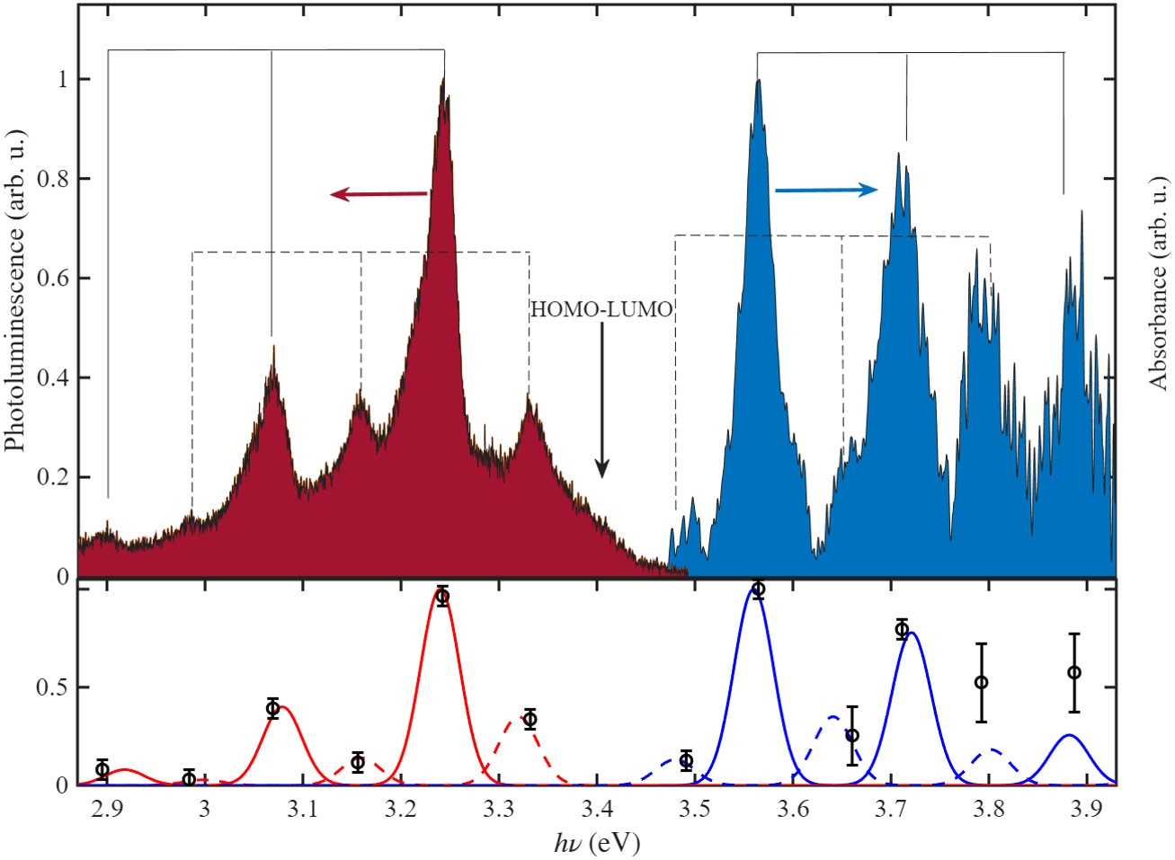
II.5 Electronic Structure and Excitonic Manifold
The excitonic landscape of the HMTP-graphene interface was probed using room-temperature photoluminescence (PL) and absorption spectroscopy (Fig. 5). PL was excited at nm using low excitation power densities to ensure the absence of photo-induced degradation. Absorption profiles were extracted via Fourier Transform Photocurrent Spectroscopy using the underlying SiC substrate as a highly sensitive internal probe. By normalizing the photo-current response of the functionalized device against the pristine SiC reference, we resolved the molecular absorption features. To account for minor setup variations during sample transfer, a smoothly varying spline background was subtracted; we verified that this procedure preserved the integrity of the spectral line shapes without introducing artificial optical responses. Both the PL and the absorption spectra exhibit a striking mirror symmetry around the HMTP monomer Highest Occupied Molecular Orbital-to-Lowest Unoccupied Molecular Orbital (HOMO-LUMO) transition, characterized by two distinct sets of transitions: a primary, high-intensity manifold and a secondary, weaker set of satellite peaks (Table 2). To contextualize these optical signatures within the broader electronic structure, we performed ARPES on the HMTP overlayer (Fig. 6). Analysis of the two major valence levels was conducted using both multi-peak Gaussian fitting and a model-unbiased Center-of-Mass (COM) integration to track the energy centroids [Fig. 6(c,d)]. The resulting dispersion is remarkably flat, with a maximum bandwidth () of only meV. Within a tight-binding framework (see Appendix E), where for the HMTP crystal geometry, we estimate the intermolecular electronic coupling () to be on the order of – meV. This small electronic bandwidth—being significantly lower than the characteristic vibrational energies (– meV) identified via Raman spectroscopy—firmly places the HMTP-graphene system in the strong electron-phonon coupling regime. In this limit, the traditional Bloch-wave description is renormalized into a set of discrete vibronic levels. The observed spectral features thus represent the transition from a non-interacting monomeric picture to the formation of Davydov-split branches, where intermolecular exchange interactions lift the degeneracy of the excitonic states into bright (bonding) and dark (antibonding) branches.


II.6 Davydov Splitting
The symmetry of the absorption and emission profiles relative to the monomer transition suggests a dominant Franck-Condon (FC) mechanism, modulated by the unique packing of the HMTP lattice. Given the intermolecular electronic coupling ( meV) is significantly smaller than the polarization energy ( meV), we describe the system using a framework of quasi-discrete vibronic levels within the strong-coupling regime [45]. As identified in the structural analysis (Fig. 4), the HMTP unit cell contains two inequivalent molecular sites. This arrangement induces the formation of bonding and anti-bonding excitonic states, lifting the degeneracy of the HOMO-LUMO transition into two Davydov-split branches separated by meV (Fig. 7) [2]. Unlike the randomized azimuthal distributions seen on amorphous supports [46], the graphene template enforces a macroscopic dipole alignment that allows us to resolve the redistribution of oscillator strength between these branches.
II.7 Absorption and the Herzberg-Teller Correction
Primary absorption, centered at 3.57 eV, corresponds to the dipole-allowed transition to the upper Davydov branch (1–0 transition). Higher-energy peaks at 3.71 eV and 3.89 eV represent subsequent phonon replicas (2–0, 3–0), characterized by the emission of meV phonons—identified in our Raman data as the Kekulé distorsion of HMTP aromatic rings. A secondary, lower-intensity set of absorption peaks (dashed lines, Fig. 5) is attributed to transitions to the lower Davydov branch. While these transitions are nominally symmetry-forbidden, the strong polaron coupling distorts the lattice sufficiently to transfer oscillator strength into these dark states. We find that the intensities of the main manifold follow a standard FC progression with a relatively small Herzberg-Teller (HT) correction - see the Appendix F for derivation. However, the minor manifold requires a larger HT correction to describe the anomalous intensity distribution.
| (1) |
where is the Huang-Rhys factor and accounts for the coordinate-dependence of the transition dipole moment and stands for emission (absorption). This HT contribution highlights the non-Franck-Condon effects introduced by the intense exciton-phonon coupling in the ordered overlayer [38].
II.8 Emission and Hot Photoluminescence
Surprisingly, the emission spectra are well-described by a pure FC mechanism (), indicating that the HT distortion is primarily an excited-state phenomenon. Following lattice relaxation to the vibronic state, polarons relax to the lower Davydov branch (blue wavy line, Fig. 7). The resulting strongest PL transition at 3.24 eV represents the 1–0 emission from this darker branch (as dictated by Kasia’s rule [20]), followed by the corresponding 160(20) meV phonon replicas. We also resolve a minor set of peaks starting at 3.33 eV, which we attribute to hot photoluminescence from the upper Davydov branch.
II.9 Quantitative Spectral Modeling
| Category | Parameter | Value | Units/Notes |
|---|---|---|---|
| Electronic Origin | Monomer Energy () | ||
| Crystal Shifts | Polarization Shift () | p m | |
| Excitonic Coupling () | p m | ||
| Vibronic Scaling | Phonon Energy () | ||
| Phonon Quanta () | 0, 1, 2 | Integer | |
| Huang-Rhys Factor () | Dimensionless | ||
| Line Broadening () | (Gaussian) | ||
| Branch Indices | Branch Index () | 1 | : Bright, : Dark |
| Weighting Factor () | Var. | Relative branch population | |
| HT Correction | Main PL Branch () | Vibronic-Induced Transition | |
| () | Minor PL Branch () | Allowed (Hot) Transition | |
| Main Abs Branch () | Weak Vibronic Mixing | ||
| Minor Abs Branch () | Forbidden (Vibronic Induced) |
To illustrate the proposed vibronic framework, we modeled the PL and absorption spectra using a series of Gaussian functions with a fixed broadening of meV to account for the experimental linewidths. The total spectral response is expressed as a sum over the two Davydov branches () and their associated phonon manifolds:
| (2) |
where the transition energies are governed by the interplay of the monomer HOMO-LUMO gap, the polarization energy , and the intermolecular exchange coupling for absorption:
| (3) |
and emission
| (4) |
In this model, represents the energy required to reconfigure the lattice upon exciton formation (the polaron shift), while signifies the Davydov splitting between the bonding and anti-bonding branches. As shown by the red (PL) and blue (absorption) curves in the bottom part of Fig. 5, this analytical approach provides an exceptional fit to the experimental data. The solid lines denote the primary dipole-allowed transitions, while the dashed lines represent the minor transitions whose intensities in absorption are dictated by the Herzberg-Teller corrected Huang-Rhys factors. The success of this fit confirms that the complex optical response of the HMTP-graphene interface can be rigorously described by a Holstein Hamiltonian parameterized solely by our independent Raman, ARPES, and structural measurements.
Our ability to resolve these intrinsic relaxation pathways [17] is a direct consequence of the interfacial order. While previous studies by Riss [33] and Chen [6] observed vibronic signatures on UHV-prepared graphene, our platform achieves a comparable level of atomic-scale definition, moreover, on a nanofabricated device. By demonstrating that the dioxolane never-dry protocol restores UHV-level LEED/LEEM purity after lithography, we bridge the gap between high-complexity device architectures and pristine surface-science models. This decoupling from the substrate minimizes lifetime broadening [33], transforming the HMTP-graphene interface into a scalable, solid-state emulator for the Holstein Hamiltonian.
III Conclusion
In summary, we have demonstrated an atomically well-defined hybrid platform that bridges the gap between scalable nanofabrication and pristine surface-science models. By implementing an all-methacrylate resist stack and a never-dry dioxolane purification protocol, we successfully recovered a UHV-equivalent graphene template on a functionalized device architecture. This structural precision allowed for the first experimental parameterization of the Holstein Hamiltonian in an HMTP-graphene system, resolved through the interplay of LEED, STM, and high-fidelity Raman mapping. Identification of the Davydov-split manifold—characterized by a splitting of and modulated by strong exciton-phonon coupling—reveals a hierarchy of bright and dark excitonic states. Crucially, the presence of symmetry-forbidden transitions from the lower Davydov branch signifies the formation of heavy, localized polarons with significantly suppressed radiative decay rates. These dark excitons represent an ideal candidate for solid-state quantum storage, as their decoupling from the radiative continuum offers a pathway toward extended coherence lifetimes in molecular-scale devices. Our platform provides a versatile tool for the next generation of organic-inorganic quantum emulators. Future work will leverage the gating capabilities of our interdigitated architecture to investigate the dynamic tuning of the Davydov splitting through external electric fields. Furthermore, the ability to maintain such high interfacial purity on pre-patterned devices opens the door for incorporating these molecular emulators into integrated photonic circuits, potentially enabling on-chip, exciton-mediated quantum information processing at room temperature.
Acknowledgements.
The financial support from the Czech Science Foundation (Grantová agentura České republiky) under project 22-04551S is gratefully acknowledged. CzechNanoLab Research Infrastructure (ID 90251), funded by MEYS CR, is gratefully acknowledged for the financial support of the measurements/sample fabrication. We also acknowledge fruitful discussions with P. Lipavský. D.V. and J.N. additionally acknowledge the support by the project Quantum Materials for Applications in Sustainable Technologies, Grant No. CZ.02.01.01/00/22_008/0004572.IV Data availability statement
The data that support the findings of this article are openly available.
Appendix A Detailed Nanofabrication Parameters

| Resist Layer | Spin Speed | Duration | Baking Temp. / Time |
|---|---|---|---|
| PMMA (AR-P 679.04) | 4000 rpm | 65 s | 200∘C / 10 min |
| MMA (AR-P 617.08) | 4000 rpm | 65 s | 200∘C / 10 min |
| MMA (AR-P 617.08) | 4000 rpm | 65 s | 180∘C / 10 min |
| Electra AR-PC 5090.02 | 4000 rpm | 65 s | 85∘C / 3 min |
| Process Step | Chemical/Medium | Duration / Conditions |
| Development: | ||
| Electra Removal | DI Water | 30 s |
| Resist Development | AR 600-56 (Methyl isobutyl ketone) | 30 s |
| Stopper | Isopropyl Alcohol (IPA) | 15 s |
| Rinse | DI Water | 15 s |
| Drying | Compressed | Until dry |
| Post-Fab Cleaning: | ||
| Primary Soak | Acetone | 2.5 h (Never-dry) |
| Rinse 1 | IPA | 30 min (Never-dry) |
| Rinse 2 | DI Water | 5 min (Never-dry) |
| Residue Removal | AR 600-71 (1,3-Dioxolane based) | 1.5 h (Never-dry) |
| Final Rinse | DI Water | 10 min (Never-dry) |
| Final Drying | Compressed | High-purity flow |
A.1 Resist Stack Engineering
The four-layer resist stack, as discussed in the main text II.1, was engineered to create a specific sensitivity gradient to optimize the undercut profile for edge-contact formation while protecting the graphene channel (Table 4).
Sensitivity Gradient: The MMA (AR-P 617.08) layers are baked at different temperatures to modulate their sensitivity to the electron beam. The MMA layer baked at 200∘C becomes more sensitive than the upper MMA layer baked at 180∘C. This creates a controlled lateral development rate, resulting in a stable, high-fidelity undercut necessary for clean metal lift-off.
The protective PMMA Base: A bottom layer of PMMA (AR-P 679.04) is critical for graphene protection. Unlike MMA, this layer acts as a sacrificial barrier that protects the graphene from over-etching during the oxygen plasma step. Because oxygen plasma etching is not perfectly directional, the absence of this layer would allow the plasma to spread beneath the MMA undercut, over-etching the graphene beyond the intended contact area restricted by a more directional metal evaporation.
A.2 E-beam Lithography and Optimization
Patterning was performed using a Raith 150-Two / Tescan Mira system at 20 kV with a beam current of 2–3 nA and a dose of 300 C/cm2 (step/line spacing: 50 nm). We found that the transition from ohmic to non-ohmic behavior is highly sensitive to both development and etching times. As shown in Fig. 8 c, oxygen plasma etching longer than 25 s results in non-ohmic contacts due to excessive lateral etching. Our optimal window was found to be 11–15 s. While the Shetty procedure uses sequential developers, our single-step development in AR 600-56 must be limited to 30 s. Extending development to 60 or 90 s, Fig. 8 d , causes the PMMA base layer to thin excessively and recede too far beneath the MMA undercut, disrupting the precise alignment of the metal evaporation with the graphene edge.
Appendix B Structural Stability of Metallization upon Thermal Annealing
To recover the pristine graphene surface for LEED and LEEM characterization, the fabricated devices must undergo a UHV outgassing procedure at 500∘C for 5 minutes II.3. While the epitaxial graphene remains inherently stable at these temperatures, it is necessary to verify the structural integrity of the wirebonding pads and interdigitated metal contacts (Ti/Cu/Au stack) for the reference sample, to ensure that the device geometry remains intact for subsequent molecular deposition and electrical probing.

As shown in Figure 9, X-ray diffraction (XRD) was employed to monitor the evolution of the metal stack—comprising 5 nm Ti, 220 nm Cu, and 20 nm Au—throughout the processing stages. X-ray coplanar diffraction () measurements were performed using a Rigaku SmartLab 3 X-ray diffractometer equipped with a rotating Cu anode (wavelength nm) and a five-circle goniometer. For this measurement, a monochromatized and collimated incident X-ray beam with a size of 0.2 mm was achieved using a parabolic multilayer mirror, followed by a 0.3 mm pinhole and a 0.2 mm collimator. The diffracted intensity was recorded using a two-dimensional detector (HyPix-3000) positioned 150 mm from the sample.
In the as-deposited state, distinct Bragg reflections corresponding to the (111) Au and (200) Cu planes are observed. Following the 500∘C annealing step, the (111) Au peak exhibits a marked reduction in intensity and significant broadening, while the (200) Cu diffraction intensity increases. These spectral shifts are characteristic of inter-diffusional alloying at the Cu-Au interface, leading to the formation of a solid solution or disordered alloy phase.
Despite this interfacial alloying, the overall morphological integrity of the leads is preserved. This is evidenced by the persistent macroscopic definition of the contacts in optical micrographs and the successful nucleation of the molecular overlayer. Upon the deposition of HMTP on the annealed contacts, a new diffraction feature emerges at the position corresponding to the (002) reflection of the HMTP molecular crystal. This confirms that the annealed metal leads remain a suitable substrate for molecular assembly. We therefore conclude that while thermal processing induces a controlled Cu-Au alloying, it does not compromise the lithographic definition or the structural stability of the device contacts.

Appendix C Graphene and HMTP Growth and Substrate-Dependent Morphology
C.1 Graphene Growth
Epitaxial graphene was synthesized by thermal decomposition of the Si-face of 4H- or 6H-SiC(0001) substrates [4] (sourced from Coherent/II-VI Inc. and Wolfspeed/Cree Inc.). The substrates mm2 were cleaned in acetone, isopropanol, and deionized (DI) water prior to loading them into the growth furnace. The growth process followed a high-temperature annealing in a purified argon atmosphere (at a pressure of mbar) to regulate the silicon sublimation rate [9, 22]. The thermal cycle consisted of sample outgassing and surface preparation at 800∘C and 1100∘C for 10 minutes each to ensure surface cleanliness and reconstruction. The final growth stage was taken at 1625-1650∘C for 5 minutes. The precise growth temperature is calibrated according to the aging of the graphite crucible, as established in our previous optimization studies [22, 34]. This calibration ensures the formation of a uniform monolayer with minimal bilayer coverage, providing the necessary atomically flat template for subsequent HMTP self-assembly.
C.2 Submonolayer HMTP Growth
All graphene samples (with and without contacts) were annealed at 530∘C for 20 min in a preparation chamber with a base pressure of (base pressure of 2 mbar). For thin film experiments, HMTP molecules were deposited in the LEEM chamber using an organic material evaporator (MBE Komponenten, Quad Cell OEZ40). The molecular powder (Merck) was kept in a resistively heated quartz crucible and operated at 170-190∘C. The LEEM chamber design results in a deposition rate that is an order of magnitude lower than in thick-layer deposition. Room-temperature Scanning Tunneling Microscopy (STM) images were obtained on a commercial system, Aarhus SPECS, using the KolibriSensor and a base pressure in the chamber of 1 mbar. Measurements were performed on a GrSiC sample without contacts using a constant current mode, the sample bias of 0.7 V, and the tunneling current of 50 pA. The contrast of the images was adjusted in Gwyddion software. Specs FE-LEEM P90 instrument was used to perform Low-Energy Electron Microscopy/Diffraction (LEEM/LEED) experiments (base pressure of 2 mbar). The bright-field images were measured by collecting electrons from the central (0,0) beam. The diffraction patterns were taken from a surface area of or using a set of apertures that reduced the beam spot on the surface to 185 nm in diameter.
C.3 Thin HMTP layers
HMTP molecules were purchased from Merck. HMTP thin films with a thickness of 50 nm were deposited using an organic molecular beam evaporator (MBE Komponenten OEZ) equipped with a resistively heated quartz crucible operated at 175∘C. The deposition was carried out in a deposition chamber with a base pressure of mbar. Prior to deposition, the substrates were cleaned by annealing at 480∘C for 5-15 minutes under ultra-high vacuum (UHV) to remove surface contaminants. The deposition rate, calibrated on pure single-layer graphene (SLG) samples using X-ray diffraction (XRD), was 5 /s. All the samples were kept at 25∘C (room temperature) during deposition, and identical growth conditions were applied for all thin film preparations.
To investigate the influence of the underlying substrate on the growth of 50 nm thin HMTP layer, discsussed in II.3, we performed high-resolution AFM topography on regions of the functional device (Fig. 10). This scale allows for a quantitative comparison of the grain boundary density and nucleation kinetics across the different material interfaces. AFM measurements were performed using a Bruker Dimension Icon microscope operated in tapping mode, and the acquired data were analyzed using Gwyddion software [31]. On the polycrystalline gold electrodes [Fig. 10(a)], the HMTP film forms a dense network of small, isotropic grains. Such a disordered landscape is expected to accelerate excitonic dephasing and localize transitions. In contrast, the morphology in the inter-electrode regions [Fig. 10(b)]—where the SiC is exposed—exhibits a distinct grain evolution. While more ordered than the growth on gold, it lacks the long-range azimuthal orientation observed on the pristine graphene template 10(c). This comparison confirms that the graphene lattice is uniquely capable of suppressing stochastic nucleation and enforcing the structural coherence.
Appendix D Macroscopic Device Alignment and HMTP Film Distribution

To confirm the spatial uniformity and precise alignment of the molecular overlayer with the underlying contact architecture, we performed large-area optical microscopy. The 50 nm thick HMTP film was deposited by thermal evaporation through a shadow mask, resulting in a well-defined molecular band across the active region of the device.
As shown in Figure 11(a), the low-magnification micrograph reveals a clear contrast difference between the pristine substrate and the deposited HMTP band (shown by blue arrows). This macro-scale verification ensures that the interdigitated electrode array is fully integrated within the functional molecular region. At higher magnification [Fig. 11(b)], the distribution of HMTP molecular aggregates is visible across the active channel. The consistent optical contrast between the metal electrodes and the SiC regions confirms that the deposition protocol allows for continuous macroscopic coverage without compromising the lithographic definition of the device leads.
Appendix E Tight-Binding Derivation of the HMTP Band Structure

To estimate the intermolecular coupling strength from our ARPES data, as we did in section II.5, we employ a nearest-neighbor tight-binding (TB) model based on the crystalline symmetry of HMTP. The unit cell contains two inequivalent molecular sites, defining two sublattices ( and ) as illustrated in Fig. 12.
E.1 Hopping Vectors and Coordination
We consider the eight primary hopping pathways for an exciton or charge carrier: six intra-sublattice neighbors within the -plane and two inter-sublattice neighbors along the -axis stacking direction. For intra-sublattice neighbors ( or ), each HMTP molecule has six neighbors in the hexagonal plane at distance :
| (5) | ||||
| (6) | ||||
| (7) |
For inter-sublattice neighbors (), the two neighbors along the -axis are at:
| (8) |
E.2 Tight-Binding Hamiltonian
The electronic states are described by the Hamiltonian matrix in the basis of the two sublattices:
| (9) |
The diagonal terms, representing the intra-sublattice dispersion, are obtained by summing the phase factors over the six in-plane neighbors:
| (10) |
with
| (11) |
The off-diagonal term represents the coupling between the two sublattices along the stacking direction:
| (12) |
E.3 Dispersion and Bandwidth
Diagonalizing yields the energy eigenvalues
| (13) |
The total bandwidth () is defined by the difference between the global maximum and minimum of the energy bands. For a simplified isotropic case where the hopping integrals are comparable (), the extrema occur at the point () and the or points (). At the point ():
At the zone boundary (namely at the point where and allows ):
| (14) |
Thus, the total theoretical bandwidth is:
| (15) |
This linear relationship allows us to directly map the meV dispersion observed in ARPES to an intermolecular coupling strength meV, confirming the heavy-exciton, strong-coupling regime.
Appendix F Vibronic Transitions and Herzberg-Teller Corrections
In this section, we provide a formal derivation of the vibronic intensity profiles, Eq. (1), based on the Franck-Condon (FC) principle and the first-order Herzberg-Teller (HT) correction. We model the system using a displaced harmonic oscillator (DHO) manifold, where the ground and excited states are represented by linear harmonic oscillators (LHO) with a relative displacement in the generalized nuclear coordinate .
F.1 Displaced Harmonic Oscillator
The generalized coordinate for a phonon mode with frequency and effective mass is expressed in terms of the bosonic creation () and annihilation () operators:
| (16) |
The displacement of the excited state potential energy surface relative to the ground state is given by , where is the dimensionless Huang-Rhys factor. We utilize the displacement operator [11] to map the ground state wavefunction onto the excited state manifold:
| (17) |
where the second equality follows from the Baker-Campbell-Hausdorff identity. The operator acts on the operators as and , shifting the expectation value of the position:
| (18) |
F.2 Franck-Condon Intensities
The transition amplitude in the Franck-Condon approximation assumes a constant electronic transition dipole moment . The intensity of the -th vibronic replica is proportional to the square of the overlap integral (Franck-Condon factor):
| (19) |
The overlap yields the well-known Poissonian distribution for intensity:
| (20) |
F.3 Herzberg-Teller Correction
To account for the coordinate dependence of the transition dipole moment, we expand to the first order [23]:
| (21) |
where . The total transition matrix element becomes:
| (22) |
Using Eq. (16), the second term is evaluated as:
| (23) |
Following the bosonic algebra for , we first identify how the displacement operator acts on the state .
| (24) |
We used the observation that in the sum; only the first two terms, , are non-zero. We can apply the second part of the displacement operator, containing the creation operator
| (25) |
Using , and , we have
| (26) |
Noticing that the second term equals , we get
| (27) |
Using the orthonormality of the LHO eigenstates, we have
| (28) |
Using Eq. (19), the first term is , and we get the final result of the matrix element
| (29) |
Combining the terms with Eq. (23), we arrive at:
| (30) |
Defining the dimensionless Herzberg-Teller coupling constant as , the final expression for the vibronic emission intensity is:
| (31) |
While the emission profile is governed by the matrix element , the absorption process requires the evaluation of the transition amplitude starting from the ground state and projecting onto the -th vibrational level of the excited state manifold. This is represented by:
| (32) |
In this case, the operator order in the second term is . Unlike the emission derivation in Eq. (23), where the commutator introduced a term, the absorption matrix element depends directly on the action of the coordinate operator on the ground state. The vibronic correction then yields a factor proportional to . Consequently, the intensity distribution for absorption, including the sign change of that stems from the operator [], is given by:
| (33) |
This formulation accounts for the non-Condon effects observed in our experimental absorption spectra, where parameterizes the vibronic borrowing strength relative to the purely electronic transition.
References
- [1] (2015) Photodegradation and self-healing in a rhodamine 6g dye and y2o3 nanoparticle-doped polyurethane random laser. Applied Physics B 120 (1), pp. 1–12. External Links: Document Cited by: §I, §II.4.
- [2] (2000) Interchain interactions in conjugated materials: the exciton model versus the supermolecular approach. Journal of Chemical Physics 112 (10), pp. 4749–4758. External Links: Document Cited by: §I, §II.6.
- [3] (1975) The infrared spectra of complex molecules. Chapman and Hall Ltd., Great Britain. Cited by: Table 1.
- [4] (2004) Ultrathin epitaxial graphite: 2d electron gas properties and a route toward graphene-based nanoelectronics. Journal of Physical Chemistry B 108 (52), pp. 19912–19916. External Links: Document Cited by: §C.1.
- [5] (2004) NIR-ft raman and ft-ir spectral studies and ab initio calculations of the anti-cancer drug combretastatin-a4. Journal of Raman Spectroscopy 35 (11), pp. 939–946. External Links: Document Cited by: Table 1.
- [6] (2013) Tuning the band gap of graphene nanoribbons synthesized from molecular precursors. ACS Nano 7 (7), pp. 6123–6128. External Links: Document Cited by: §I, §I, §II.9.
- [7] (2024) How accurate are simulations and experiments for the lattice energies of molecular crystals?. Physical Review Letters 133 (4), pp. 046401. External Links: Document Cited by: §II.4.
- [8] (2004) Intramolecular and low-frequency intermolecular vibrations of pentacene polymorphs as a function of temperature. Journal of Physical Chemistry B 108 (6), pp. 1822–1826. External Links: Document Cited by: Table 1, Table 1.
- [9] (2009) Towards wafer-size graphene layers by atmospheric pressure graphitization of silicon carbide. Nature Materials 8 (3), pp. 203–207. External Links: Document Cited by: §C.1.
- [10] (2020) A unification of the holstein polaron and dynamic disorder pictures of charge transport in organic crystals. Physical Review X 10 (2), pp. 021062. External Links: Document Cited by: §I.
- [11] (1951) An operator calculus having applications in quantum electrodynamics. Physical Review 84 (1), pp. 108–128. External Links: Document Cited by: §F.1.
- [12] (2025) A new approach to molecular and lattice simulations with crystalmaker® 11. MRS Communications 15 (5), pp. 1007–1016. External Links: Document Cited by: §II.4.
- [13] (2023) A comprehensive approach to exciton delocalization and energy transfer. Journal of Chemical Theory and Computation 19 (2), pp. 436–447. External Links: Document Cited by: §I, §I.
- [14] (2011) Interaction of charge carriers with lattice and molecular phonons in crystalline pentacene. Journal of Chemical Physics 135 (8), pp. 084701. External Links: Document Cited by: Table 1, Table 1.
- [15] (2018) Engineering vibrationally assisted energy transfer in a trapped-ion quantum simulator. Physical Review X 8 (1), pp. 011038. External Links: Document Cited by: §I.
- [16] (2013) Where does it vibrate? raman spectromicroscopy on a single molecule. Angewandte Chemie International Edition. External Links: Document Cited by: §I, §II.4.
- [17] (2006) Effect of disorder on ultrafast exciton dynamics probed by single molecule spectroscopy. Physical Review Letters 97 (21), pp. 216403. External Links: Document Cited by: §I, §II.9.
- [18] (2012) On-chip quantum simulation with superconducting circuits. Nature Physics 8 (4), pp. 292–299. External Links: Document Cited by: §I.
- [19] (2020) Surface-controlled crystal alignment of naphthyl end-capped oligothiophene on graphene: thin-film growth studied by in situ x-ray diffraction. Langmuir 36 (8), pp. 1898–1906. External Links: Document Cited by: §I.
- [20] (1956) Molecular electronic spectroscopy. Annual Review of Physical Chemistry 7, pp. 403–424. External Links: Document Cited by: §II.8.
- [21] (2012) Absorption, circular dichroism, and photoluminescence in perylene diimide bichromophores: polarization-dependent h- and j-aggregate behavior. Journal of Physical Chemistry B 116 (1), pp. 77–86. External Links: Document Cited by: §I, §I.
- [22] (2017) Effect of residual gas composition on epitaxial growth of graphene on sic. Physical Review Applied 8 (4), pp. 044011. External Links: Document Cited by: §C.1.
- [23] (2022) Franck-condon and herzberg-teller signatures in molecular absorption and emission spectra. Journal of Physical Chemistry B 126 (15), pp. 2899–2911. External Links: Document Cited by: §F.3.
- [24] (2013) Jet spectroscopy of buckybowl: electronic and vibrational structures in the s0 and s1 states of triphenylene and sumanene. Journal of Chemical Physics 139 (4), pp. 044313. External Links: Document Cited by: §II.4, Table 1, Table 1.
- [25] (1990) Resonance raman enhancement of phenyl ring vibrational-modes in phenyl iron complex of myoglobin. Biophysical Journal 57 (4), pp. 851–856. External Links: Document Cited by: Table 1, Table 1.
- [26] (2019) Vibration-assisted exciton transfer in molecular aggregates strongly coupled to confined light fields. Journal of Chemical Physics 150 (10), pp. 105102. External Links: Document Cited by: §I.
- [27] (2016) A scalable clean graphene transfer process using polymethylglutarimide as a support scaffold. Journal of The Electrochemical Society 163 (6), pp. E159–E161. External Links: Document Cited by: §I.
- [28] (2010) Molecular structure, spectroscopic (ftir, ftir gas phase, ft-raman) first-order hyperpolarizability and homo-lumo analysis of 4-methoxy-2-methyl benzoic acid. Journal of Raman Spectroscopy 41 (10), pp. 1369–1378. External Links: Document Cited by: Table 1.
- [29] (2012) Digital quantum simulation of the holstein model in trapped ions. Physical Review Letters 109 (20), pp. 200501. External Links: Document Cited by: §I.
- [30] (1977) Structure of 1,1’-diethyl-2,2’-cyanine iodide, a photographic sensitizing dye. Acta Crystallographica Section B 33, pp. 2181–2188. External Links: Document Cited by: §I.
- [31] (2012) Gwyddion: an open-source software for spm data analysis. Central European Journal of Physics 10 (1), pp. 181–188. External Links: Document Cited by: §C.3.
- [32] (2011) The effect of chemical residues on the physical and electrical properties of chemical vapor deposited graphene transferred to sio2. Applied Physics Letters 99 (12), pp. 122108. External Links: Document Cited by: §I, §II.3.
- [33] (2014) Imaging and tuning molecular levels at the surface of a gated graphene device. ACS Nano 8 (6), pp. 5395–5401. External Links: Document Cited by: §I, §II.9.
- [34] (2025) Annealing, design and long-term operation of graphite crucibles for the growth of epitaxial graphene on sic. Journal of Crystal Growth 651, pp. 127988. External Links: Document Cited by: §C.1.
- [35] (2023) Scalable fabrication of edge contacts to 2d materials: implications for quantum resistance metrology and 2d electronics. ACS Applied Nano Materials 6 (7), pp. 6292–6298. External Links: Document Cited by: §II.1.
- [36] (1980) Infrared characteristic group frequencies. John Wiley & Sons, Great Britain. Cited by: §II.4, Table 1, Table 1, Table 1, Table 1, Table 1, Table 1, Table 1, Table 1, Table 1, Table 1, Table 1, Table 1, Table 1, Table 1, Table 1, Table 1, Table 1, Table 1.
- [37] (2010) Photodegradation and aggregation of acridine dyes adsorbed on the surface of mesoporous tio2 films. Journal of Applied Spectroscopy 77 (2), pp. 202–205. External Links: Document Cited by: §I, §II.4.
- [38] (2014) Molecular packing versus strength and effective mass of the emitting exciton of -1,1,4,4-tetraphenyl-1,3-butadiene. Journal of Physical Chemistry C 118 (16), pp. 8588–8594. External Links: Document Cited by: §I, §II.7.
- [39] (2006) Dynamics of the intermolecular transfer integral in crystalline organic semiconductors. Journal of Physical Chemistry A 110 (11), pp. 4065–4070. External Links: Document Cited by: Table 1.
- [40] (2022) Ultra-clean high-mobility graphene on technologically relevant substrates. Nanoscale 14 (6), pp. 2167–2176. External Links: Document Cited by: §I, §II.2, §II.2.
- [41] (2026) Crystal ordering of an organic semiconductor imposed by two weakly interacting substrates - hmtp on graphene and native oxide/sic. To be submitted. Cited by: §I.
- [42] (2026) Interfacial coupling controls molecular epitaxy of hmtp on graphene/sic. External Links: 2601.22263, Link Cited by: §I, §II.3.
- [43] (2020) Recent advances in graphene patterning. ChemPlusChem 85 (8), pp. 1655–1668. External Links: Document Cited by: §I.
- [44] (2010) Ultrafast dynamics of frenkel excitons in tetracene and rubrene single crystals. Journal of Physical Chemistry C 114 (23), pp. 10580–10591. External Links: Document Cited by: §I.
- [45] (2011) Influence of vibronic coupling on band structure and exciton self-trapping in -perylene. Journal of Physical Chemistry B 115 (18), pp. 5157–5167. External Links: Document Cited by: §I, §II.6.
- [46] (2008) Molecular beam deposition and characterization of thin organic films on metals for applications in organic electronics. Physica Status Solidi A 205 (3), pp. 497–510. External Links: Document Cited by: §I, §II.6.
- [47] (2015) High mobility epitaxial graphene devices via aqueous-ozone processing. Applied Physics Letters 106 (6), pp. 063503. External Links: Document Cited by: §I.
- [48] (2010) Far-infrared spectroscopy of cationic polycyclic aromatic hydrocarbons: zero kinetic energy photoelectron spectroscopy of pentacene vaporized from laser desorption. Astrophysical Journal 715 (1), pp. 485–492. External Links: Document Cited by: Table 1.