A 200 dB Dynamic Range Radiation‑Hard Delta‑Sigma Current Digitizer for Beam Loss Monitoring
Abstract
This paper presents a radiation-hardened current-mode delta-sigma ADC fabricated in a standard 130 nm CMOS technology and qualified for total ionizing doses up to 100 Mrad. The converter is designed for beam loss monitoring applications in high-energy physics, where it must handle input currents spanning nine decades, from 1 mA down to 1 pA, while providing a fast 10 µs response time for machine protection. To meet these conflicting requirements, the architecture exploits the inherent trade-off between resolution and acquisition time: a first-order modulator sampled at 20 MHz delivers 11-bit effective resolution within the critical 10 µs window for the mA current range. Extended integration times of up to 100 s enable the sub-picoampere resolution required for beam alignment and background monitoring and provides an operational dynamic range exceeding 200 dB. The chip integrates two independent channels, consumes 25 mW from a 1.2 V supply, and includes radiation-hardening techniques such as triple-redundant digital logic and SEU-tolerant comparator banks. Post-irradiation measurements up to 100 Mrad show no performance degradation, and the uncalibrated integral nonlinearity remains within [+0.2%, –0.3%] of full scale over the 1 mA to 5 µA range. The converter’s flexibility and radiation tolerance make it suitable not only for the HL-LHC beam loss monitoring upgrade but also for other precision current measurement applications in harsh environments.
I Introduction
RADIATION-TOLERANT current digitizers primarily find their use in harsh environments where radiation monitoring is required, like in high energy physics experiments and nuclear power plants. For example, at CERN the radiation levels are carefully monitored around the Large Hadron Collider in order to protect the machine components and to accurately position the absorber jaws of the mechanical beam collimation system. In both cases the sensing element is a gas filled ionization chamber [1, 2, 3] that produces a fixed charge rate when subject to constant radiation levels; the corresponding electrical signal ranges from 1 mA to few picoamperes (pA) that represent respectively the maximum tolerable radiation energy, which absorbed within the response time of the beam dumping system, and the typical background radiation levels. Various current sensing interfaces exist either built with discrete components [4] or as integrated circuits [5]; in any case their radiation tolerance limit imposes a lower bound for the length of the cable connecting the interface with the sensor. Long cables limit the detection dynamic range due to interference, noise charge associated with the parasitic capacitance and leakage current. The radiation levels around the LHC are maximum at the collimators preceding the interaction points (IP3 and IP7) [6] and are expected to grow after the High Luminosity upgrade foreseen by 2025. The radiation around the collider originates from the losses of the beams circulating inside the machine, since the relevant quantity is the dose rate absorbed within one turn rather than its instantaneous value, the application band of interest spans from dc up to 12 kHz. An integrated radiation tolerant frontend has therefore been developed to comply with the stringent requirements of radiation monitoring in harsh environments. To this end a standard CMOS 130 nm technology was selected after being successfully characterized to tolerate a total ionizing dose (TID) of 200 Mrad [7, 8, 9] when adopting specific radiation hardness measures to prevent latch up, drain/source leakage and to tolerate SEU and SET in the digital parts. The remainder of this manuscript is organized as follows. Section II presents the system requirements and design drivers derived from the Beam Loss Monitoring application and the HL-LHC upgrade constraints. Section III describes the architecture of the proposed delta-sigma current digitizer, discussing its resolution limit and stability considerations while also providing the foundational concepts for readers less familiar with this architecture. Section IV details the circuit-level implementation, including the integrator, quantizer, adaptive clock control and DAC. Section V reports the experimental results, including noise performance, linearity, and dynamic range as a function of acquisition time, for samples irradiated with X-rays up to 100 Mrad. Finally, Section VI concludes the paper.
II System Requirements and Design Drivers
| Requirement | Value — Range | Design Driver — Origin |
|---|---|---|
| Input Current Range |
1 pA to 1 mA
(180 dB) |
Ionization chamber physics: dynamic range spans from minimum detectable losses for beam alignment to full-scale quench-inducing events. |
|
Response time for
currents |
10 µs | Beam dump response time: the system must react within 10 µs to trigger a beam bump and prevent sub-systems damage and magnet quenching. |
|
Radiation Tolerance
(tested survival) |
Mrad
(1 MGy) |
HL-LHC radiation level projections: electronics must survive the integrated dose expected over the upgraded accelerator lifetime. |
| Technology Node | CMOS 130 nm | CERN-qualified process for 200 Mrad tolerance; offers optimal balance between radiation hardness, analog performance, density, and power. |
| Supply Voltage |
1.2 V (thick-oxide devices
compatible with 2.5 V) |
Standard for 130 nm CMOS; trade-off between power consumption, signal swing, and noise performance. |
|
Number of Channels
per Chip |
2 analog readout channels | System density: approximately 4000 ionization chambers served by 750 acquisition modules, resulting in 3 to 4 ASICs per module. |
|
Cable Length
Compatibility |
Coaxial up to 50 m | Tunnel infrastructure: long connections between chambers and electronics introduce attenuation and filtering. Proximity to high radiation accelerates aging. |
|
Communication
Protocol |
LpGBT
(e-Link compatible) |
Compatibility with HL-LHC data aggregation and timing distribution infrastructure. |
|
Communication
Redundancy |
Dual communication
channels |
System reliability: ensure continuous operation and data transmission even in case of link failure. |
|
Radiation-Induced
Errors |
SEU resilience
(TRM a digital design) |
High-energy hadron fluxes expected in HL-LHC tunnel; mitigation of single-event upsets is mandatory. |
| EMI Immunity |
Robust against
electromagnetic interference |
Harsh accelerator environment with high-power RF systems, switching transients and non-negligible magnetic fields. |
|
Out-of-Range Input
Handling |
Operational for currents
beyond nominal range |
Ensures collider protection: system remains responsive during extreme events and recovers without latch-up or damage. |
|
Chip Physical
Dimensions |
Fits within 64-pin QFP cavity; balances functionality, power dissipation, and mechanical robustness. |
-
a
Triple redundant modular design with majority voting and spatial spread.
The Beam Loss Monitoring (BLM) system [10] is a critical protection element of the LHC accelerator complex, designed to prevent quenches of superconducting magnets and equipment damage caused by excessive radiation following beam misalignment. The system continuously measures radiation levels along the accelerator using approximately 4000 ionization chambers installed throughout the 27 km of the circular collider. When ionizing radiation passes through the gas-filled chambers, the resulting charge is extracted by a high-voltage bias of 1.5 kV and converted into a current signal proportional to the instantaneous beam loss. In the original LHC design these signals are transmitted via coaxial cables, up to 800 m in length, to about 750 acquisition modules for processing and analysis.
To ensure compatibility with the higher luminosity and correspondingly increased radiation levels expected from the HL-LHC upgrade, a new generation of front-end electronics must meet stringent performance, reliability, and environmental constraints. The enhanced radiation tolerance enables the readout electronics to be installed closer to the sensors, thereby improving signal integrity. However, depending on the radiation levels and associated aging effects, the electronics must also remain compatible with cable lengths of up to 50 m to preserve installation flexibility, although with relaxed requirements for the non-critical current levels ().
Another critical requirement is the response time for triggering an emergency beam dump. The beam circulation time inside the machine is , and the electronics must be capable of initiating a dump within of detecting a fault condition. Table I summarizes the key system-level requirements and the design drivers that shape the ASIC architecture.
The stringent requirements of a nine-decade dynamic range and a response time would imply impractically high instantaneous resolution for a direct conversion approach. However, this requirement can be relaxed when considering the limited signal bandwidth of and the variable acquisition time, which can extend up to tens or even hundreds of seconds for non-critical currents. This long-acquisition, high-resolution regime corresponds to beam alignment tracking, where the signals can be considered essentially static. Consequently, the first-order current-mode delta-sigma ADC emerges as an ideal candidate for beam loss monitoring applications. While higher-order modulators offer superior noise shaping and can achieve higher resolution for a given oversampling ratio, their performance advantage diminishes for near-DC signals, where the effective resolution is ultimately limited by the DC gain of the loop filter—a parameter that is comparable to that of a first-order modulator for a given amplifier gain. Moreover, their stability is more complex and less robust, particularly under saturation or overload conditions, where they are prone to prolonged recovery transients or latch-up. In contrast, the first-order architecture provides predictable, unconditional stability and graceful saturation recovery, making it ideally suited for a machine protection system where reliability and deterministic behavior are paramount.
The extreme radiation requirement, exceeding 100 Mrad TID, dictates both technology choice (130 nm CMOS) and design methodology. Digital circuits must be triplicated with majority voting to mitigate single-event upsets (SEUs), while analog blocks require manual enclosed layout and larger guard rings to remain functional after cumulative dose degradation.
The use of long cable, extending up to 50 m, adds substantial capacitance to the ionization chamber’s intrinsic 350 pF, bringing the total load seen by the front-end to 5 nF. This extended capacitance demands a low input impedance to mitigate cable-induced time constants, while also requiring the circuit to withstand the noise and interference inevitably picked up over such transmission lengths.
Finally, the system’s role as a machine protection element imposes absolute reliability requirements. Redundant communication channels, SEU mitigation, and graceful out-of-range behavior are not optional but mandatory to ensure the BLM system can fulfill its critical function throughout the HL-LHC operational lifetime.
III Converter architecture

The core of the measurement system is a continuous-time, first-order, single-bit delta-sigma modulator, which converts the sensor’s input current into a digital bitstream. A simplified schematic of this ADC is shown in Figure 4.
The front-end of the modulator consists of an active integrator, which serves two critical purposes: it collects the ionization charge generated by the sensor over time and acts as a filter for the feedback loop. The integrator’s output is continuously monitored by a comparator, clocked at a default frequency of 20 MHz derived by dividing the 80 MHz clock used for the digital circuitry. This frequency represents the optimal trade-off between the integrator’s bandwidth and the analog-to-digital conversion range achievable within the 10 µs response time. On each clock edge, the integrator output is compared to a reference threshold, effecting both sampling and 1-bit quantization. The comparison result drives a time-varying negative feedback loop that prevents the integrator from saturating. This feedback is implemented via a 1-bit digital-to-analog converter (DAC), consisting of a current source and a switch controlled by the comparator’s output. The precision of the compensation charge depends on the stability of the reference current and the clock period. The effectiveness of the sigma-delta conversion relies on the continuous accumulation of the net difference between the input and feedback signals, and on its attenuation by the loop filter gain. A high DC loop gain guarantees that the time-averaged compensation signal closely follows the average input current. To first order, therefore, the achievable resolution of the converter is proportional to the DC gain of the integrator.
The bitstream produced by the quantizer is the digital representation of the compensation signal whose average value is directly encoded in the density of ’1’s within this bitstream. For static inputs, therefore, the upper bound of the achievable resolution is given by the number of distinguishable codes, expressed as:
| (1) |
where is the sampling frequency and is the acquisition time per measurement. The relationship is depicted in Figure 2
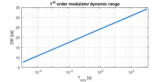
Eq. 1 highlights the intrinsic trade-off between signal bandwidth and conversion resolution characteristic of the sigma-delta topology, making it ideally suited for accurate, high-resolution measurements of slowly varying signals. The bandwidth limitation comes from using longer bitstreams to evaluate the instantaneous average.
III-A Decimation filtering
The raw bitstream retains the large quantization error inherent to single-bit quantization, which encodes only the sign of the integrator output relative to a threshold. Under the action of the loop-filter, however, this error is attenuated at low frequencies and it’s energy content is shaped toward the higher end of the spectrum. Figure 3 illustrates the effect of the integrator’s finite gain-bandwidth product on the modulator’s noise-shaping characteristic.

In this regime, the excess quantization error can be removed through real-time filtering of the bitstream. The industry standard is an n-th order sinc filter whose transfer function is:
| (2) |
where M is the bitstream length and n the number of cascaded first-order stages. The case n=1 correspond to a simple moving average, representing the sweet spot for low latency and hardware efficiency, while n=3 provides optimal accuracy. This low-pass filtering also enables the symbol rate to be reduced accordingly without any loss of information.
The inherent trade-off between accuracy and bandwidth offered by sigma-delta conversion can be further exploited by making the outputs of these multiple filter stages available simultaneously. Thereby allowing the BLM system to concurrently use measurement with varying bandwidth and resolution for optimal beam alignment and collimation.
III-B Non-idealities
Beyond the usual limitations of analog components such as noise, offset, slew rate, finite gain-bandwidth, quantizer delay, and switch non-idealities, the converter architecture itself introduces notable non-idealities.
One such phenomenon is the appearance of limit cycles when the static input current approaches a rational multiple of the compensation signal. Under these conditions, the bitstream exhibits periodic regularity, concentrating quantization error energy at specific frequencies in the output spectrum. However, this effect is not critical: as zero-mean tones, their primary impact, if not properly mitigated, is a potential 1-bit oscillation between consecutive output samples.
A second issue arises from transient upsets—such as radiation-induced single-event upsets (SEUs) or out-of-range inputs—that drive the integrator into saturation. During saturation, the bitstream locks to a constant sequence of ’1’s, causing a temporary spill of quantization error into lower frequencies until recovery is complete and normal operation resumes.
Finally although converter overload triggers an emergency beam dump it should be noted that unless an ESD protection discharge occurs, the ionization chamber charge is conserved and eventually absorbed and correctly measured by the converter.
III-C 1-st order modulator stability
A first-order delta-sigma modulator presents an interesting perspective on stability. From a linear control systems standpoint, the modulator is unconditionally stable: its single-pole loop filter yields a well-behaved step response with no tendency toward oscillation or unbounded growth.
On the other hand, the system can also be viewed as inherently unstable in the sense that a DC input does not produce a DC output. Instead, it generates a continuous high-frequency modulation that, crucially, remains non-periodic for most input values. This non-periodic behavior arises from the sharp nonlinearity introduced by the 1-bit quantizer, whose transfer characteristic is effectively discontinuous (resembling a staircase). Far from being pathological, this irregular oscillation is the fundamental mechanism underlying noise shaping which spreads the quantization error across the upper portion of the spectrum, preventing its concentration into discrete tones.
This apparent paradox stems from the fact that the modulator is not a strictly linear time-invariant (LTI) system as it comprises a nonlinear quantizer and time-varying elements in the switched feedback current. Nevertheless, the system can be approximated as quasi-LTI to a useful extent, allowing feedback theory considerations to remain applicable as a first-order approximation.

IV Circuit implementation
Building upon the operational principles of the delta-sigma modulator, this section delves into the circuit-level realization of the converter. This approach highlights how system-level considerations such as noise performance, power consumption, and bandwidth are translated into concrete circuit topologies and device-level decisions.
The main architectural features of the analog-to-digital converter implemented on silicon are shown in Figure 4. The integrator employs a fully differential topology, which converts the single-ended, unipolar signal from the sensor into a differential representation. This conversion results from the interaction between the integration path, which charges exclusively the upper output node, and the common mode regulation, which induces a complementary current in the lower integration capacitor to stabilize the output common mode. This approach provides an increased output swing and enhanced immunity to on-chip digital interference. To optimize power consumption and accuracy, an adaptive clock control scheme is implemented, scaling the operating frequency for smaller input signals. The compensation current source is steered using complementary switches, minimizing transient settling errors and improving overall accuracy.
IV-A Amplifier
At the heart of the fully differential integrator lies the operational transconductance amplifier (OTA), the most critical analog block in the signal chain. Its performance directly governs the overall linearity, noise, and settling behavior of the modulator, ultimately determining the achievable resolution of the converter.
The amplifier, shown in Figure 5, employs a fully differential, two-stage, cascode-compensated topology with a rail-to-rail output stage capable of class-AB operation. The first stage is implemented as a folded cascode using a PMOS input pair, which provides high gain and good common-mode rejection. The choice of PMOS devices for the input pair is motivated by their lower susceptibility to radiation-induced flicker noise increase, as their buried conduction channel is less affected by damage at the interface with the gate oxide.
The differential output is realized with a push-pull configuration, biased through a translinear loop to precisely control its quiescent current.
The design is adapted from [11] and optimized for the integrator requirements. It achieves an open-loop gain exceeding 95 dB, a unity-gain bandwidth above 50 MHz, and a phase margin of 74 degrees. The input-referred offset is 0.62 mV, while the total current consumption remains below 4 mA from a 1.2 V supply. The thermal output noise level is 3.6 nV/ with a flicker corner frequency around 20 kHz. The amplifier’s high DC gain ensures effective attenuation of quantization noise at low frequencies, while its unity-gain bandwidth strikes an ideal compromise between settling speed and noise performance. The class-AB configuration prevents slew-rate limitations during large-signal excursions without incurring excessive power penalty.

IV-B Quantizer
The 1-bit quantizer, Figure 6, is implemented as a synchronous comparator using a strong-arm latch topology, which is reset during the low phase of the clock and released on its rising edge. The total current drawn from the supply—before the comparator is fully steered—is limited by a tunable bias current programmable from 160 to with 3-bit resolution. This bias current also influences the comparison speed and noise performance.
The comparator output generates a control signal for the compensation current, which remains active for a full clock cycle—from the current rising edge until the next. This approach optimizes the correction current sizing by relying on the well-controlled clock period rather than its duty cycle.
To enhance the system’s radiation hardness, a selectable triple-redundant comparator configuration can be enabled. In this mode, three parallel comparators are activated, and a majority voting logic circuit produces the final output.
The comparator achieves, in the minimum current configuration, an input-referred offset of , an input-referred noise of , and exhibits a transient voltage kickback of 175 mV.
IV-C Adaptive clock control
The dynamic clock rate control is a feature designed to minimize switching activity in the proximity of the analog circuitry when small currents are being measured. The clock control logic monitors the output bitstream and adjusts the clock frequency—ranging from 20 MHz down to 38 Hz—based on the number of consecutive identical symbols detected. The on-pulse duration remains fixed, as it determines the value of the compensation charge together with the reference current. The clock rate is doubled or halved depending on which string of identical symbols is observed.
The modulator’s optimal operating mode is found in the neighborhood of the middle of the input range, where the commutation rate is maximized and the quantization error is uniformly spread across the spectrum. The length of consecutive symbols required to trigger a clock rate change drives a trade-off between the response time of the additional control loop, the target switching activity, and the interaction with the signal dynamics. This threshold is programmable and is typically set to three consecutive symbols after allowing sufficient time for the modulator to settle.
For a given static current, the minimum operating frequency is determined by the value that would cause the integrator to saturate within two clock cycles.
To mitigate the long settling time following a large input step, an asynchronous comparator is introduced. It monitors the integrator output and resets the clock to its maximum frequency if saturation is detected, thereby overriding the dynamic control loop and ensuring a fast response on the order of tens of microseconds.
IV-C1 Asynchronous comparator
The asynchronous comparator, Figure 7, is implemented as a two-stage open-loop amplifier with a total gain of 43 dB. The first stage is a low-gain preamplifier designed to reduce kickback toward the integrator; it employs a common-source topology with resistive loads. The second stage features a regenerative cross-coupled load that guarantees rapid decision-making through positive feedback. Diode-connected loads prevent saturation, thereby ensuring a faster recovery.
The comparator monitors only the negative integrator output and compares it to an internal threshold voltage. This threshold is generated by steering a bandgap-derived current of through an adjustable resistor producing reference voltages from 10 to 300 mV. The comparator exhibits an input-referred offset of 2.2 mV and a hysteresis of 7 mV provided by the positive feedback. Its current consumption is .


IV-D DAC
The feedback signal is generated by a 1-bit DAC, which can be trimmed using a 5-bit control word to adjust the converter’s full-scale range according to the expected input current, spanning from to . In order to prevent the modulator from saturating, the feedback current must be at least one LSB larger than the maximum input current.
The total output-referred noise of the DAC is .Relating this to its nominal output and expressing the ratio in bits yields:
| (3) |
This contribution, however, does not limit conversion accuracy in the mid and lower signal ranges. Because the modulator scales a fixed compensation current with the input, the associated noise scales proportionally. As a result, the DAC’s effective noise diminishes with decreasing input current and is further reduced by bitstream averaging. The DAC is implemented as a current mirror using NMOS devices, incorporating cascode transistors and degeneration resistors to enhance noise performance. To prevent radiation-induced mismatch, unused devices are kept active by continuously drawing current from the common-mode voltage (Vcm), rather than being switched off.

V Measurements Results
The ASICs were irradiated without their package lids, using CERN’s in-house 50 kV, 3 kW X-ray generator (SEIFERT RP149). The total accumulated dose reached 100 Mrad, with an absorbed dose rate of approximately 8.82 Mrad/h referred to . During irradiation, the chips were operated under worst-case conditions: a supply voltage of 1.575 V (approximately 30% above nominal), a sampling frequency of 20 MHz, and a static input current of 1 mA, while the operating temperature was maintained at 25 °C.
Post-irradiation performance characterization was carried out on a separate test bench, with annealing occurring only passively during storage at room temperature for a few hours: a scenario representative of realistic operating conditions. No measurable performance degradation was observed; any differences between pre- [13, 12] and post-irradiation measurements were indistinguishable from statistical variation.
Input currents down to 1 pA were generated using a calibrated source-measure unit with guarded triaxial connections (Keithley 6430 equipped with remote amplifier module). Special care was taken in the PCB design to further reduce leakage [13], including the use of shielding and minimizing the distance between connectors and the ASIC to about 2 cm.
Data acquisition was carried out using a BLM crate housing a VFC acquisition board, capable of storing up to 2 Gbit raw bit-stream per measurement. The acquired data were then exported to a PC for post-processing. Each measurement corresponds to a fixed DC input current. The equivalent noise current is evaluated as a function of acquisition time by subdividing the raw bitstream into smaller, consecutive segments. For each segment, the average density of ’1’s is computed, and the noise is then taken as the standard deviation of these repeated measurements. The equivalent input referred noise current assumes Figure 11 reports the equivalent input-referred noise as a function of acquisition time for input currents spanning from 1 mA down to 10 pA. The most relevant measurement combinations are detailed in Table II indicates that sub-pA accuracy requires a minimum of ten seconds of integration and input currents below 10 nA. The dominant noise source shifts with current levels; as predicted by simulations, the compensation DAC limits accuracy at higher current ranges, while the operational amplifier dominates at lower ranges. Grayed-out cells in the table indicate incompatible parameter combinations for which the noise exceeds the targeted measurement range. By relating the maximum static input current to the minimum noise level observed over a 100 s integration window, the resulting operating dynamic range is:
| (4) |
However, this value is only attainable across multiple input ranges, as the noise contribution from the compensation current scales with the square root of the density of ’1’s in the bitstream. Table III presents the measured ENOB as a function of the integration time and input current. With a integration window, 11-bit effective resolution is achieved only for the highest current. At 100 ms, however, 15-bits accuracy extends over three decades, from to 1 mA. For 100 s, 15 bits are exceeded for currents spanning from 1 mA down to 10 nA.
The ADC transfer characteristic and its integral non-linearity (INL) were evaluated for the fastest acquisition setting (Figure 12). With a 20 MHz sampling frequency, this configuration yields 200 distinct output codes within the integration window. Over the corresponding input range, , the uncalibrated INL remains within +0.2% and -0.3% of full scale in compliance with the BLM application requirements.


| Input Current | Integration Time | |||||||
|---|---|---|---|---|---|---|---|---|
| 10 s | 100 s | 1 s | 10 s | 100 s | 1 s | 10 s | 100 s | |
| 1 A | 400 A | 60 A | 30 A | 28 A | 26 A | 23 A | 20 A | 18 A |
| 100 A | 600 A | 60 A | 7 A | 4 A | 2.8 A | 2.3 A | 2.2 A | 2 A |
| 10 A | 200 A | 60 A | 6 A | 2.2 A | 300 A | 230 A | 220 A | 200 A |
| 1 A | 500 A | 60 A | 5 A | 600 A | 60 A | 22 A | 20 A | 13 A |
| 100 A | 200 A | 60 A | 4 A | 600 A | 60 A | 6 A | 2 A | 1.8 A |
| 10 A | 60 A | 20 A | 4 A | 600 A | 60 A | 6 A | 0.6 A | 130 A |
| 1 A | 20 A | 7 A | 2 A | 600 A | 60 A | 6 A | 0.6 A | 130 A |
| 100 A | 10 A | 3 A | 1 A | 300 A | 60 A | 6 A | 0.6 A | 80 A |
| 10 A | 5 A | 2 A | 600 A | 200 A | 60 A | 6 A | 0.6 A | 80 A |
| Input Current | |||
|---|---|---|---|
| 1 A | 11.28 | 15.23 | 15.76 |
| 100 A | 7.38 | 15.12 | 15.61 |
| 10 A | 5.64 | 15.02 | 15.61 |
| 1 A | – | 14.02 | 16.23 |
| 100 A | – | 10.70 | 15.76 |
| 10 A | – | 7.38 | 16.23 |
| 1 A | – | 4.05 | 12.90 |
| 100 A | – | – | 10.28 |
| 10 A | – | – | 6.96 |
The power consumption of the 2-channel ASIC is below 25 mW from a single 1.2 V supply.
VI Conclusion
This paper has presented a radiation-tolerant current digitizer ASIC designed for beam loss monitoring applications in the HL-LHC environment. The architecture is derived directly from stringent system-level requirements, including a wide input dynamic range (1 mA to 1 pA), short integration windows (down to 10 µs), deterministic overload recovery, and tolerance to total ionizing doses exceeding 100 Mrad.
A first-order delta-sigma topology was selected to ensure unconditional stability, predictable saturation behavior, and robustness under large transient inputs, as required in machine protection systems. The achievable dynamic range scales with the product of sampling frequency and acquisition time, enabling high resolution for quasi-static signals while preserving fast response capability. In 10 µs mode, the system achieves 11-bit resolution, while extended acquisition enables significantly higher effective resolution for low-level signals.
The circuit implementation in a 130 nm CMOS process incorporates radiation-hardening techniques at both architectural and layout levels. Experimental results demonstrate correct functionality and no measurable performance degradation after exposure to 100 Mrad under worst-case bias conditions. Noise measurements confirm pA-level resolution, and linearity results validate correct operation across the full input range.
The proposed approach demonstrates that wide dynamic range, deterministic behavior, and high radiation tolerance can be simultaneously achieved within a compact monolithic solution. Although developed for the LHC Beam Loss Monitoring system, the architecture is applicable to other high-radiation and wide-dynamic-range current sensing applications in high-energy physics and related fields
Acknowledgments
The author would like to thank the CERN EP-ESE Group and the BE-BI Group for their contribution to the development of this work. Special thanks are due to Jan Kaplon for his invaluable support in analog ASIC design and exquisite mentorship, to Pedro Leitao for the design of the digital part, to Giulio Borghello for assistance with irradiation tests, to Francesco Martina for the PCB design and to Christos Zamantzas for providing access anf thechnical support to the BL testing laboratory.
References
- [1] Stockner, Markus, et al. ”Measurements and simulations of ionization chamber signals in mixed radiation fields for the LHC BLM system.” 2006 IEEE Nuclear Science Symposium Conference Record. Vol. 3. IEEE, 2006.
- [2] Theis, C., et al. ”Characterisation of ionisation chambers for a mixed radiation field and investigation of their suitability as radiation monitors for the LHC.”Radiation protection dosimetry 116.1-4 (2005): 170-174.
- [3] Dehning, B., et al. ”Classification of the LHC BLM Ionization Chamber.” (2007).
- [4] Vigano, William, et al. ”10 orders of magnitude current measurement digitisers for the CERN beam loss systems.” Journal of Instrumentation 9.02 (2014): C02011-C02011.
- [5] Voulgari, Evgenia, et al. ”Utopia: A nine decade femtoampere sensitivity current digitizer and its application in ionizing radiation monitoring.” IEEE Transactions on Nuclear Science 65.3 (2018): 932-940.
- [6] Lerner, G., R. Garcìa Alìa, and K. Bilko. ”Radiation level specifications for HL-LHC.” CERN, Geneva, Switzerland, Rep. CERN-EDMS 2302154 (2020).
- [7] Faccio, F., et al. ”Radiation-induced short channel (RISCE) and narrow channel (RINCE) effects in 65 and 130 nm MOSFETs.” IEEE Transactions on Nuclear Science 62.6 (2015): 2933-2940.
- [8] Gonella, L., et al. ”Total ionizing dose effects in 130-nm commercial CMOS technologies for HEP experiments.”Nuclear Instruments and Methods in Physics Research Section A: Accelerators, Spectrometers, Detectors and Associated Equipment 582.3 (2007): 750-754.
- [9] Borghello, Giulio, et al. ”Dose-rate sensitivity of 65-nm MOSFETs exposed to ultrahigh doses.” IEEE Transactions on Nuclear Science 65.8 (2018): 1482-1487
- [10] Holzer, Eva Barbara, et al. Design of the beam loss monitoring system for the LHC ring. No. LHC-Project-Report-781. 2004.
- [11] Hogervorst, Ron, et al. ”A compact power-efficient 3 V CMOS rail-to-rail input/output operational amplifier for VLSI cell libraries.” IEEE journal of solid-state circuits 29.12 (2002): 1505-1513.
- [12] Martina, Francesco, et al. ”Testbed Development for the Characterisation of an ASIC for Beam Loss Measurement Systems.” (2020): THPP04.
- [13] Martina, Francesco, et al. ”JACoW: Methodology, Characterisation and Results from the Prototype Beam Loss Monitoring ASIC at CERN.” JACoW IBIC 2021 (2021): 294-298.