Influence of excitation energy on microscopic quantum pathways for ultrafast charge transfer in van der Waals heterostructures
Abstract
Efficient charge separation in van der Waals (vdW) heterostructures is crucial for optimizing light harvesting and detection applications. However, precise control over the microscopic pathways governing ultrafast charge transfer remains an open challenge. These pathways are intrinsically linked to charge transfer states with strongly delocalized wave functions that appear at various momenta in the Brillouin zone. Here, we use time- and angle-resolved photoemission spectroscopy (trARPES) to investigate the possibility of steering carriers through specific charge transfer states in a prototypical WS2-graphene heterostructure. By selectively exciting electron-hole pairs at the K-point (A-exciton resonance) and close to the Q-point (C-exciton resonance) of WS2 with different pump photon energies, we find that charge separation is faster at higher excitation energies. This behavior is attributed to the fact that absorption at the C-exciton resonance generates electron-hole populations at energies well above the direct band gap. The resulting elevated carrier temperatures open an additional, highly efficient charge-transfer channel for holes in the WS2 valence band, leading to an overall acceleration of interlayer hole transfer for C-exciton excitation. The microscopic insights gained in this work can be leveraged to optimize the performance of vdW heterostructures in optoelectronic devices.
I Introduction
The vast selection of 2D materials available today, such as graphene and monolayer transition metal dichalcogenides, enables the design of novel heterostructures with tailored properties [1, 2, 3]. Such heterostructures commonly feature efficient absorption of visible light followed by ultrafast charge separation [4, 5, 6, 7, 8, 9, 10] with great potential for applications in light harvesting and detection. The driving force behind ultrafast charge separation is the band alignment, where photoexcited electrons and holes rapidly relax to the conduction band minimum and valence band maximum in separate layers. Charge transfer states, formed by hybridization between the vdW-coupled layers, create delocalized wave functions that serve as ultrafast tunneling channels [11, 12, 13]. These states occur at various momenta and energies in the Brillouin zone but do not contribute equally to charge separation. Based on existing models [11, 13, 14, 15, 16, 17, 18], the efficiency of different tunneling channels depends on the strength of the hybridization, the size of the energy barriers that photo-excited carriers must overcome to reach the charge transfer state, as well as the available tunneling phase space. The possibility to steer carriers through specific charge transfer states, e.g. by selectively generating them at particular momenta and with controlled excess energies, remains unexplored.
Here, we investigate this concept in a prototypical vdW heterostructure consisting of monolayer WS2 and graphene. We photoexcite the heterostructure with pump photon energies of and to excite electron-hole pairs at the K-point (A-exciton) and between the - and Q-point (C-exciton) of WS2, respectively, and probe the charge transfer dynamics directly in the band structure using time- and angle-resolved photoemission spectroscopy (trARPES) [19]. We find that charge separation is significantly faster following excitation, which we attribute to the activation of a second, highly efficient charge transfer channel in the valence band. Our findings introduce new possibilities for optimizing charge separation in vdW heterostructures, paving the way for more efficient light-harvesting and detection technologies.
II Methods
Sample growth: Pretreated 4H-SiC substrates were H-etched to remove scratches and graphitized in Ar atmosphere. The resulting carbon monolayer with structure was decoupled from the SiC substrate by H-intercalation, yielding quasi-freestanding monolayer graphene [20]. WS2 was then grown by chemical vapour deposition (CVD) from solid WO3 and S precursors [21, 22]. Both graphene and WS2 growth were monitored using Raman spectroscopy, atomic force microscopy and secondary electron microscopy. WS2 was found to grow in the shape of triangular islands with side lengths in the range of with twist angles of either 0° or 30° with respect to the graphene layer [13].
trARPES: The setup was based on a Ti:Sa amplifier (Astrella, Coherent) with repetition rate, pulse duration, photon energy, and output power. Of this, were frequency-doubled and used to drive high harmonics generation (HHG) in an Argon gas jet. The 7th harmonic at was isolated using a grating monochromator and focused onto the sample with a beam diameter of . A small part of the output was frequency doubled to generate pump pulses with a photon energy of with a fluence of at the focus. The remaining seeded an optical parametric amplifier (Topas Twins, Light Conversion). One of the signal beams was frequency doubled to generate pump pulses with a photon energy of with a fluence of at the focus. The photoemitted electrons were detected with a hemispherical analyzer (Phoibos 100, SPECS) to obtain snapshots of the occupied band structure along the K direction of graphene. The temporal and energy resolutions were and , respectively.
III Results
Figure 1a shows an ARPES image of the WS2-graphene heterostructure at negative pump-probe delay before the arrival of the pump pulse. The dotted, dashed, and continuous lines indicate the theoretical band structures of WS2 islands with a twist angle of 0°, WS2 islands with a twist angle of 30° [23] and graphene [24], respectively. The bands are shifted in energy to fit the experimentally observed band alignment and doping level. Orange and blue arrows mark the electronic transitions in WS2 excited at and , respectively [25]. Here, we will only consider WS2 islands with 0° twist angle. The influence of the twist angle on ultrafast charge separation will be investigated in a separate work.
Figure 1b depicts the pump-induced changes of the photocurrent in Fig. 1a after photoexcitation at with a fluence of . Brown and blue colors indicate a gain and loss of photoelectrons, respectively, with respect to negative pump-probe delay. Figure 1c is the same as Fig. 1b but for photoexcitation at with a fluence of and after photoexcitation. For both excitation energies we observe gain in the conduction band (CB) of WS2, gain (loss) above (below) the equilibrium Fermi level in graphene, and a complex gain-loss signal in the WS2 valence band (VB) with contributions from band shifts and broadening as previously discussed in [18, 13].
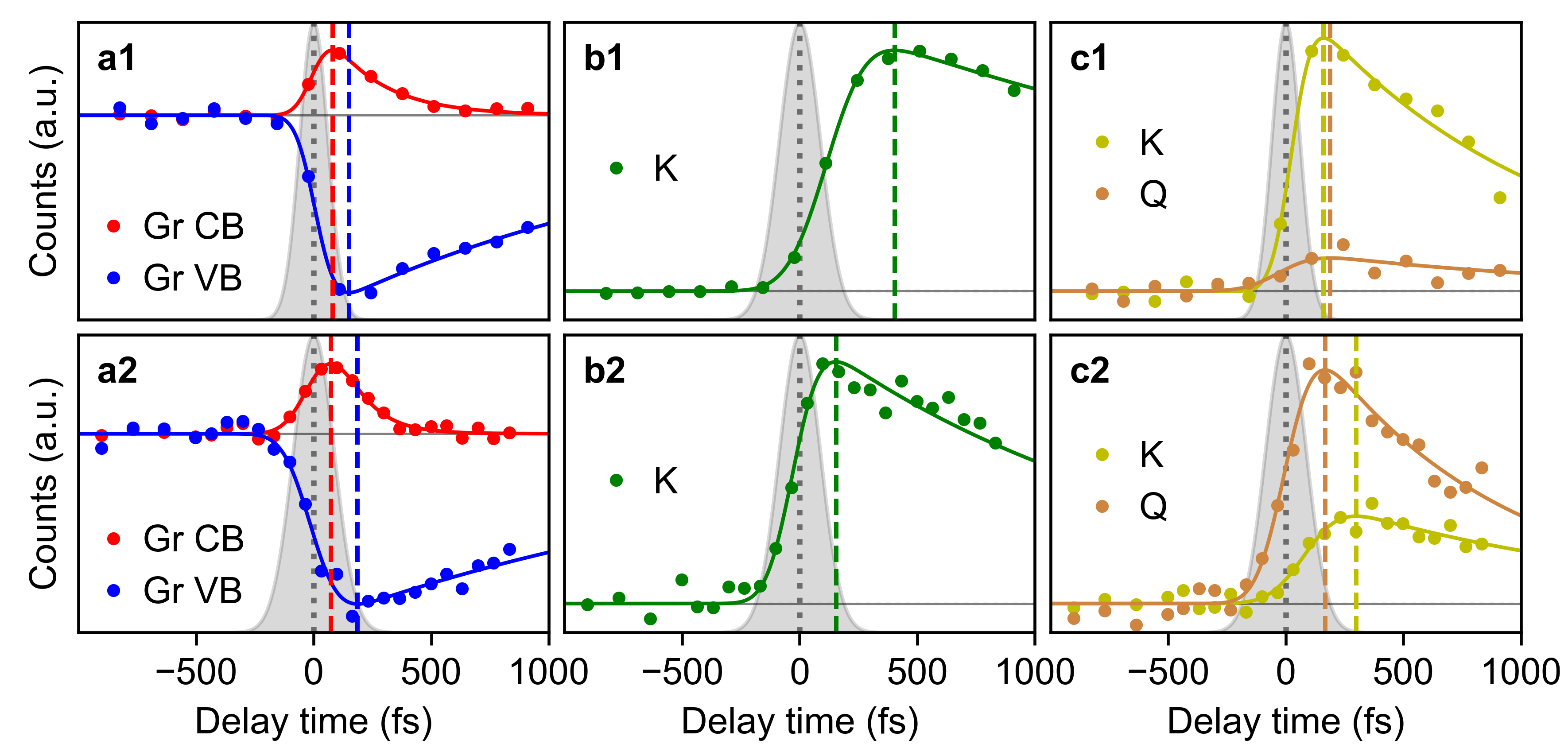
To gain access to the transient carrier population of different parts of the band structure, we integrate the photocurrent over the areas marked by the colored boxes in Figs. 1b and c. The corresponding pump-probe traces are shown in Fig. 2 together with single-exponential fits (see supplemental material) yielding the decay times . Dashed vertical lines in Fig. 2 indicate the pump-probe delay where the respective pump-probe trace reaches its extremum. The fit results are summarized in Table 1. The charge carrier dynamics inside the Dirac cone (Fig. 2a) are found to be quite similar for and , respectively, considering that the pump-pulse cross-correlation (grey-shaded areas in Fig. 2) was longer for () than for (). The population dynamics of the WS2 bands, however, show important differences when comparing the two excitation energies. We find that the gain above the equilibrium position of the WS2 VB (Fig. 2b) reaches its maximum later for than for . Further, for , the pump-probe signal of the WS2 CB at K is much bigger than close to Q, indicating that the photoexcited electrons are mainly confined to the K valley (Fig. 2c1). For , however, we find that the population of the WS2 CB at K is smaller than the one close to Q and reaches its maximum later (Fig. 2c2).
To gain direct access to the timescales for ultrafast charge separation, we extract the related charging-induced band shifts of the WS2 VB and CB as follows [18, 13]. First, we extract energy distribution curves (EDCs) at selected momenta from the trAPRES snapshots in Fig. 1 that we fit with an appropriate number of Gaussian peaks (see supplemental material) to obtain the transient binding energies shown in Fig. 3a. Next, we subtract the transient position of the WS2 VB from the transient position of the WS2 CB yielding the transient band gap shown in Fig. 3b. Finally, assuming that the band gap changes symmetrically around its center, we add (subtract) half of the transient band gap change to (from) the transient position of the WS2 VB (CB) to obtain the shifts in Fig. 3c that we previously attributed to a transient charging of the WS2 layer with excess electrons [18, 13].
The corresponding charging shift of the graphene layer in Fig. 3d is obtained by extracting momentum distribution curves (MDCs) that we fit with a Lorentzian (see supplemental material). The resulting peak positions are averaged and multiplied with the slope of the Dirac cone to yield the data points in Fig. 3d. All orange and blue curves in Fig. 3 are single-exponential fits (see supplemental material), the fit parameters of which are summarized in Table 2. Vertical dashed orange and blue lines indicate the positions , where the respective pump-probe signals reach their extrema. Note that the fit for the transient band gap in Fig. 3b is sensitive to the value assumed for the equilibrium gap size (we assumed ) which also affects in Fig. 3c. We would like to stress, though, that varying the equilibrium gap size by a reasonable amount has only a minor influence on the data points in Fig. 3c. Considering this, the behavior of the transient WS2 band gap at is very similar for and . In contrast to this, both the WS2 and the graphene charging shifts are found to depend on the pump photon energy. We find that both charging shifts reach their extrema later for than for .
IV Discussion
The results obtained for are in good agreement with previous trARPES results [26, 18, 13] making their interpretation straight forward. The asymmetric population dynamics of the Dirac cone (Fig. 2a1), the gain above the equilibrium position of the WS2 VB (Fig. 2b1) and the charging shifts in Figs. 3c and d provide direct evidence of ultrafast charge separation in the WS2-graphene heterostructure, where hole transfer from WS2 to graphene is much faster than electron transfer. The relevant charge transfer states for the WS2-graphene heterostructure have been previously identified using density functional theory calculations [13]. For convenience, we sketch the relevant part of the band structure in Fig. 4. Charge transfer states, where the WS2 and graphene bands hybridize, are shown in red. For , photoexcitation occurs at the K valley of WS2. The previously proposed scattering processes resulting in ultrafast charge transfer to the graphene layer are indicated by orange arrows [18, 13]. The transient reduction of the band gap in Fig. 3b has been previously attributed to screening of the Coulomb interaction by photoinduced free carriers [27, 28, 29, 30, 31, 32, 19].
The observed differences between excitation at and , however, deserve further discussion. We start with the observation that, for , the population dynamics in the WS2 CB in Fig. 2c2 are different at K and close to Q. The pump pulse directly populates states close to the Q valley (see Fig. 1a) [25]. These carriers are then observed to scatter to the K valley within (see Fig. 2c2) in good agreement with previously reported intervalley scattering times for WS2 and similar TMDCs [33, 34, 35, 36, 37].
Next, we focus on the observation that the gain above the equilibrium position of the WS2 VB (Fig. 2b) and the charging shifts (Fig. 3c and d) are found to reach their extrema at earlier time delays for than for . This indicates that hole transfer is faster for than for . From [18] it is known that the rates for charge transfer from WS2 to graphene increase with increasing electronic temperature as it becomes easier for the photoexcited carriers to overcome the energy barriers to the closest charge transfer states.
The transient electronic temperature for the WS2 layer is difficult to determine due to the limited signal-to-noise ratio. Therefore, we estimate the peak electronic temperatures for electrons and holes in WS2 as described in detail in the supplemental material. We obtain as the excess energy of the carriers is considerably larger at . This, indeed, makes it easier for the holes to overcome the energy barrier (see Fig. 4). In addition, is high enough for the holes to reach the second charge transfer state at in the VB with an energy barrier of . Hole transfer at is expected to be faster than at because the size of the avoided crossing between WS2 VB and graphene Dirac cone is bigger (and therefore hybridization is stronger) [13]. The excitation and charge transfer channels for are indicated by blue arrows in Fig. 4.
Note that the photoexcited carrier densities (an estimate is provided in the supplementary material) exceed the Mott threshold [28, 38, 39], where photoexcited excitons rapidly decay into free electron-hole pairs. Therefore, we believe excitonic effects to be irrelevant for interpreting our trARPES data.
Finally, we would like to briefly comment on the possible influence of ultrafast energy transfer between WS2 and graphene. Following photoexcitation of vdW heterostructures, both charge and energy transfer are possible relaxation channels. While the charging shifts in our data provide direct evidence of ultrafast charge separation and thus ultrafast charge transfer, indications for ultrafast energy transfer are less obvious. Note that our data shows none of the indications of Meitner-Auger energy transfer discussed in [40]. A possible contribution of Förster energy transfer [41] is difficult to evaluate from our data. However, we would like to point out that the presence or absence of additional energy transfer does not affect our conclusions regarding ultrafast charge transfer.
V Summary and Outlook
In summary, we used trARPES of a WS2-graphene heterostructure to show that the elevated carrier temperature following C-exciton excitation activates a second, highly efficient charge transfer channel for holes. These results show that charge separation across vdW interfaces can be controlled via the incident pump photon energy, opening up new strategies to optimize the performance of vdW heterostructures for future applications in light harvesting and detection.
VI Acknowledgments
This work received funding from the European Union’s Horizon 2020 research and innovation program under Grant Agreement No. 851280-ERC-2019-STG (DANCE) and No. 101130384 (QUONDENSATE), from the German Research Foundation (DFG) via the Collaborative Research Centre 1277 (Project No. 314695032) and the Research Unit 5242 (Project No. 449119662), as well as from the German Federal Ministry of Education and Research (BMBF) (Project No. 05K2022).
References
- Geim and Grigorieva [2013] A. K. Geim and I. V. Grigorieva, Van der Waals heterostructures, Nature 499, 419 (2013).
- Novoselov et al. [2016] K. S. Novoselov, A. Mishchenko, A. Carvalho, and A. H. Castro Neto, 2D materials and van der Waals heterostructures, Science 353, 461 (2016).
- Jin et al. [2018] C. Jin, E. Y. Ma, O. Karni, E. C. Regan, F. Wang, and T. F. Heinz, Ultrafast dynamics in van der Waals heterostructures, Nature Nanotechnology 13, 994 (2018).
- He et al. [2014] J. He, N. Kumar, M. Z. Bellus, H. Y. Chiu, D. He, Y. Wang, and H. Zhao, Electron transfer and coupling in graphene-tungsten disulfide van der Waals heterostructures, Nature Communications 5, 5622 (2014).
- Massicotte et al. [2016] M. Massicotte, P. Schmidt, F. Vialla, K. G. Schädler, A. Reserbat-Plantey, K. Watanabe, T. Taniguchi, K. J. Tielrooij, and F. H. Koppens, Picosecond photoresponse in van der Waals heterostructures, Nature Nanotechnology 11, 42 (2016).
- He et al. [2017] J. He, D. He, Y. Wang, and H. Zhao, Probing effect of electric field on photocarrier transfer in graphene-WS2 van der Waals heterostructures, Optics Express 25, 1949 (2017).
- Ji et al. [2017] Z. Ji, H. Hong, J. Zhang, Q. Zhang, W. Huang, T. Cao, R. Qiao, C. Liu, J. Liang, C. Jin, L. Jiao, K. Shi, S. Meng, and K. Liu, Robust Stacking-Independent Ultrafast Charge Transfer in MoS2/WS2 Bilayers, ACS Nano 11, 12020 (2017).
- Song et al. [2018] Z. Song, H. Zhu, W. Shi, D. Sun, and S. Ruan, Ultrafast charge transfer in graphene-WS2 Van der Waals heterostructures, Optik 174, 62 (2018).
- Yuan et al. [2018] L. Yuan, T. F. Chung, A. Kuc, Y. Wan, Y. Xu, Y. P. Chen, T. Heine, and L. Huang, Photocarrier generation from interlayer charge-transfer transitions in WS2-graphene heterostructures, Science Advances 4, e1700324 (2018).
- Fu et al. [2021] S. Fu, I. du Fossé, X. Jia, J. Xu, X. Yu, H. Zhang, W. Zheng, S. Krasel, Z. Chen, Z. M. Wang, K. J. Tielrooij, M. Bonn, A. J. Houtepen, and H. I. Wang, Long-lived charge separation following pump-wavelength–dependent ultrafast charge transfer in graphene/WS2 heterostructures, Science Advances 7, eabd9061 (2021).
- Zheng et al. [2017] Q. Zheng, W. A. Saidi, Y. Xie, Z. Lan, O. V. Prezhdo, H. Petek, and J. Zhao, Phonon-Assisted Ultrafast Charge Transfer at van der Waals Heterostructure Interface, Nano Letters 17, 6435 (2017).
- Liu et al. [2022] J. Liu, X. Zhang, and G. Lu, Auger Processes and Excited State Dynamics in WS2/Graphene Heterostructures: A First-Principles Perspective, Journal of Physical Chemistry Letters 13, 7371 (2022).
- Hofmann et al. [2023] N. Hofmann, L. Weigl, J. Gradl, N. Mishra, G. Orlandini, S. Forti, C. Coletti, S. Latini, L. Xian, A. Rubio, D. Perez Paredes, R. Perea Causin, S. Brem, E. Malic, and I. Gierz, Link between interlayer hybridization and ultrafast charge transfer in WS2-graphene heterostructures, 2D Materials 10, 035025 (2023).
- Wang et al. [2016] H. Wang, J. Bang, Y. Sun, L. Liang, D. West, V. Meunier, and S. Zhang, The role of collective motion in the ultrafast charge transfer in van der Waals heterostructures, Nature Communications 7, 11504 (2016).
- Long and Prezhdo [2016] R. Long and O. V. Prezhdo, Quantum Coherence Facilitates Efficient Charge Separation at a MoS2/MoSe2 van der Waals Junction, Nano Letters 16, 1996 (2016).
- Li et al. [2017] L. Li, R. Long, and O. V. Prezhdo, Charge Separation and Recombination in Two-Dimensional MoS2/WS2: Time-Domain ab Initio Modeling, Chemistry of Materials 29, 2466 (2017).
- Liu et al. [2021] Y. Liu, J. Zhang, S. Meng, C. Yam, and T. Frauenheim, Electric Field Tunable Ultrafast Interlayer Charge Transfer in Graphene/WS2Heterostructure, Nano Letters 21, 4403 (2021).
- Krause et al. [2021] R. Krause, S. Aeschlimann, M. Ch, M. Chavez-Cervantes, R. Perea-Causin, S. Brem, E. Malic, S. Forti, F. Fabbri, C. Coletti, and I. Gierz, Microscopic understanding of ultrafast charge transfer in van-der-Waals heterostructures, Physical Review Letters 127, 276401 (2021).
- Hofmann et al. [2025] N. Hofmann, A. Steinhoff, R. Krause, N. Mishra, G. Orlandini, S. Forti, C. Coletti, T. O. Wehling, and I. Gierz, k-Resolved Ultrafast Light-Induced Band Renormalization in Monolayer WS2 on Graphene, Nano Letters 25, 1214 (2025).
- Riedl et al. [2009] C. Riedl, C. Coletti, T. Iwasaki, A. A. Zakharov, and U. Starke, Quasi-free-standing epitaxial graphene on SiC obtained by hydrogen intercalation, Physical Review Letters 103, 246804 (2009).
- Rossi et al. [2016] A. Rossi, H. Büch, C. Di Rienzo, V. Miseikis, D. Convertino, A. Al-Temimy, V. Voliani, M. Gemmi, V. Piazza, and C. Coletti, Scalable synthesis of WS2 on graphene and h-BN: An all-2D platform for light-matter transduction, 2D Materials 3, 031013 (2016).
- Forti et al. [2017] S. Forti, A. Rossi, H. Büch, T. Cavallucci, F. Bisio, A. Sala, T. O. Menteş, A. Locatelli, M. Magnozzi, M. Canepa, K. Müller, S. Link, U. Starke, V. Tozzini, and C. Coletti, Electronic properties of single-layer tungsten disulfide on epitaxial graphene on silicon carbide, Nanoscale 9, 16412 (2017).
- Zeng et al. [2013] H. Zeng, G. B. Liu, J. Dai, Y. Yan, B. Zhu, R. He, L. Xie, S. Xu, X. Chen, W. Yao, and X. Cui, Optical signature of symmetry variations and spin-valley coupling in atomically thin tungsten dichalcogenides, Scientific Reports 3, 1608 (2013).
- Wallace [1947] P. R. Wallace, The Band Theory of Graphite, Physical Review 71, 622 (1947).
- Magnozzi et al. [2020] M. Magnozzi, M. Ferrera, G. Piccinini, S. Pace, S. Forti, F. Fabbri, C. Coletti, F. Bisio, and M. Canepa, Optical dielectric function of two-dimensional WS2 on epitaxial graphene, 2D Materials 7, 025024 (2020).
- Aeschlimann et al. [2020] S. Aeschlimann, A. Rossi, M. Chávez-Cervantes, R. Krause, B. Arnoldi, B. Stadtmüller, M. Aeschlimann, S. Forti, F. Fabbri, C. Coletti, and I. Gierz, Direct evidence for efficient ultrafast charge separation in epitaxial WS2/graphene heterostructures, Science Advances 6, eaay0761 (2020).
- Ugeda et al. [2014] M. M. Ugeda, A. J. Bradley, S. F. Shi, F. H. Da Jornada, Y. Zhang, D. Y. Qiu, W. Ruan, S. K. Mo, Z. Hussain, Z. X. Shen, F. Wang, S. G. Louie, and M. F. Crommie, Giant bandgap renormalization and excitonic effects in a monolayer transition metal dichalcogenide semiconductor, Nature Materials 13, 1091 (2014).
- Chernikov et al. [2015] A. Chernikov, C. Ruppert, H. M. Hill, A. F. Rigosi, and T. F. Heinz, Population inversion and giant bandgap renormalization in atomically thin WS2 layers, Nature Photonics 9, 466 (2015).
- Ulstrup et al. [2016] S. Ulstrup, A. G. Čabo, J. A. Miwa, J. M. Riley, S. S. Grønborg, J. C. Johannsen, C. Cacho, O. Alexander, R. T. Chapman, E. Springate, M. Bianchi, M. Dendzik, J. V. Lauritsen, P. D. King, and P. Hofmann, Ultrafast Band Structure Control of a Two-Dimensional Heterostructure, ACS Nano 10, 6315 (2016).
- Pogna et al. [2016] E. A. Pogna, M. Marsili, D. De Fazio, S. Dal Conte, C. Manzoni, D. Sangalli, D. Yoon, A. Lombardo, A. C. Ferrari, A. Marini, G. Cerullo, and D. Prezzi, Photo-induced bandgap renormalization governs the ultrafast response of single-layer MoS2, ACS Nano 10, 1182 (2016).
- Cunningham et al. [2017] P. D. Cunningham, A. T. Hanbicki, K. M. McCreary, and B. T. Jonker, Photoinduced Bandgap Renormalization and Exciton Binding Energy Reduction in WS2, ACS Nano 11, 12601 (2017).
- Lin et al. [2022] Y. Lin, Y. H. Chan, W. Lee, L. S. Lu, Z. Li, W. H. Chang, C. K. Shih, R. A. Kaindl, S. G. Louie, and A. Lanzara, Exciton-driven renormalization of quasiparticle band structure in monolayer MoS2, Physical Review B 106, L081117 (2022).
- Wallauer et al. [2016] R. Wallauer, J. Reimann, N. Armbrust, J. Güdde, and U. Höfer, Intervalley scattering in MoS2 imaged by two-photon photoemission with a high-harmonic probe, Applied Physics Letters 109, 162102 (2016).
- Bertoni et al. [2016] R. Bertoni, C. W. Nicholson, L. Waldecker, H. Hübener, C. Monney, U. De Giovannini, M. Puppin, M. Hoesch, E. Springate, R. T. Chapman, C. Cacho, M. Wolf, A. Rubio, and R. Ernstorfer, Generation and Evolution of Spin-, Valley-, and Layer-Polarized Excited Carriers in Inversion-Symmetric WSe2, Physical Review Letters 117, 277201 (2016).
- Dong et al. [2021] S. Dong, M. Puppin, T. Pincelli, S. Beaulieu, D. Christiansen, H. Hübener, C. W. Nicholson, R. P. Xian, M. Dendzik, Y. Deng, Y. W. Windsor, M. Selig, E. Malic, A. Rubio, A. Knorr, M. Wolf, L. Rettig, and R. Ernstorfer, Direct measurement of key exciton properties: Energy, dynamics, and spatial distribution of the wave function, Natural Sciences 1, e10010 (2021).
- Wallauer et al. [2021] R. Wallauer, R. Perea-Causin, L. Münster, S. Zajusch, S. Brem, J. Güdde, K. Tanimura, K. Q. Lin, R. Huber, E. Malic, and U. Höfer, Momentum-Resolved Observation of Exciton Formation Dynamics in Monolayer WS2, Nano Letters 21, 5867 (2021).
- Bange et al. [2023] J. P. Bange, P. Werner, D. Schmitt, W. Bennecke, G. Meneghini, A. A. AlMutairi, M. Merboldt, K. Watanabe, T. Taniguchi, S. Steil, D. Steil, R. T. Weitz, S. Hofmann, G. S. Jansen, S. Brem, E. Malic, M. Reutzel, and S. Mathias, Ultrafast dynamics of bright and dark excitons in monolayer WSe2 and heterobilayer WSe2MoS2, 2D Materials 10, 035039 (2023).
- Steinhoff et al. [2017] A. Steinhoff, M. Florian, M. Rösner, G. Schönhoff, T. O. Wehling, and F. Jahnke, Exciton fission in monolayer transition metal dichalcogenide semiconductors, Nature Communications 8, 1166 (2017).
- Siday et al. [2022] T. Siday, F. Sandner, S. Brem, M. Zizlsperger, R. Perea-Causin, F. Schiegl, S. Nerreter, M. Plankl, P. Merkl, F. Mooshammer, M. A. Huber, E. Malic, and R. Huber, Ultrafast Nanoscopy of High-Density Exciton Phases in WSe2, Nano Letters 22, 2561 (2022).
- Dong et al. [2023] S. Dong, S. Beaulieu, M. Selig, P. Rosenzweig, D. Christiansen, T. Pincelli, M. Dendzik, J. D. Ziegler, J. Maklar, R. P. Xian, A. Neef, A. Mohammed, A. Schulz, M. Stadler, M. Jetter, P. Michler, T. Taniguchi, K. Watanabe, H. Takagi, U. Starke, A. Chernikov, M. Wolf, H. Nakamura, A. Knorr, L. Rettig, and R. Ernstorfer, Observation of ultrafast interfacial Meitner-Auger energy transfer in a Van der Waals heterostructure, Nature Communications 14, 5057 (2023).
- Tebbe et al. [2024] D. Tebbe, M. Schütte, K. Watanabe, T. Taniguchi, C. Stampfer, B. Beschoten, and L. Waldecker, Distance Dependence of the Energy Transfer Mechanism in WS2 -Graphene Heterostructures, Physical Review Letters 132, 196902 (2024).
- Erben et al. [2022] D. Erben, A. Steinhoff, M. Lorke, and F. Jahnke, Optical nonlinearities in the excited carrier density of atomically thin transition metal dichalcogenides, Physical Review B 106, 045409 (2022).


| Red box | Blue box | Yellow box | Orange box | ||
| Graphene | |||||
| gain | Graphene | ||||
| loss | Gain above | ||||
| equilibrium position | |||||
| of WS2 VB | Gain in WS2 | ||||
| CB at K | Gain in WS2 | ||||
| CB close to Q | |||||
| fs | ps | 3.2 p m 0.4 | ps | ps | |
| fs | ps | 1.5 p m 0.1 | ps | ps | |
| fs | fs | ∼400 | fs | fs | |
| fs | fs | ∼160 | fs | fs |
| WS2 VB position | ΔE_charge^WS2 | |||
| ps | ps | 2.7 p m 0.9 | ps | |
| meV | meV | 110 p m 10 | meV | |
| ps | ps | 1.5 p m 0.2 | ps | |
| meV | meV | 127 p m 6 | meV | |
| fs | fs | ∼540 | fs | |
| fs | fs | ∼200 | fs |
Influence of excitation energy on microscopic quantum pathways for ultrafast charge transfer in van der Waals heterostructures
SUPPLEMENTAL MATERIAL
VII Exponential decay fits
To extract rise and decay times of a given pump-probe signal, we use the following analytic fitting function that stems from convolving a step function with exponential decay for the underlying dynamics with a Gaussian accounting for the finite temporal resolution:
| (1) |
Here, is the amplitude, is the error function, is the full width at half maximum of the Gaussian, is the time delay where pump and probe overlap, and is the decay time. This function was used to fit the time traces in Figs. 2 and 3 in the main manuscript.
VIII Extracting transient peak positions
For extracting the transient position of the WS2 valence band, the data in Fig. 1a (main manuscript) were integrated over the momentum range for and for around . The latter was chosen to ensure that the graphene valence band does not influence the data. The resulting energy distribution curves (EDCs) were then fitted with a constant background and three Gaussian peaks for the three expected bands. Exemplary fits are presented in Fig. 5a. The following constraints were applied:
-
•
The constant background was fixed to the value found for negative pump-probe delay.
-
•
The energy difference between the two spin-split WS2 valence bands was fixed to the value found for negative pump-probe delay.
-
•
The spectral weight of bands 1 and 2 was fixed to the value found for negative pump-probe delay.
To obtain the transient position of the WS2 conduction band, the data in Fig. 1b and c (main manuscript) were integrated over the momentum range around . The resulting EDCs were then fitted with a background-free Gaussian (see Fig. 5b).
The shift of the graphene Dirac cone was determined by integrating the data in Fig. 1a (main manuscript) over the energy range around the five energy positions . To improve the signal-to-noise ratio, we grouped the resulting momentum distribution curve (MDC) data into bins of three consecutive time delays. The final MDCs were fitted by the sum of a constant background and a Lorentzian peak (see Fig. 5c) for every energy position. The five momentum shifts obtained in this way were averaged and then converted into an energy shift by multiplying with the slope of the -band of .

IX Estimating transient carrier temperatures in WS2
According to [42], the absorption in the relevant fluence regime is highly non-linear. The excited carrier density for resonant excitation of the C-exciton with a fluence of can be directly obtained from [42] as . [42] also showed that absorption at the A-exciton resonance drops to zero when similar carrier densities are reached. Therefore, we assume that both and excitation generate carrier densities on the order of even though the incident fluences differ considerably.
To estimate the peak carrier temperature, we first assume that the excess energy for electrons and holes can be directly converted into a carrier temperature . The excess energy for excitation is yielding . The A-exciton resonance, however, lies below the single-particle gap. In our case, the photoexcited carrier densities exceed the Mott threshold, such that the excitons rapidly decay into free electron-hole pairs. These free electron-hole pairs screen the Coulomb interaction which results in a transient reduction of the single particle band gap by (see Fig. 3b of main manuscript). Therefore, it seems justified to assume that, for excitation, electrons and holes gain an excess energy of yielding a transient carrier temperature of .
An improved estimate can be obtained by calculating the carrier temperature in the framework of the quasi-free electron model. Here, the change of the internal energy due to heating of a given carrier density from room temperature to an arbitrary temperature is given by
where the 2D . and are the spin and valley degeneracies, respectively. From the carrier concentration we obtain the chemical potential that, in Sommerfeld approximation, is independent of temperature. The part of the absorbed fluence that is available for heating the carriers is given by the product of the photoexcited carrier density and the excess energy . From we obtain and for an effective mass of .