

Artificial Spin Ice Phase-Change Memory Resistors
Abstract
We study the implications of the anisotropic magnetic resistance on permalloy nanowires, and in particular on the property of the resistance depending on the type of lattice. We discuss how the internal spin configuration of artificial spin ice nanowires can affect their effective resistive state, and which mechanisms can introduce a current-dependent effect dynamic resistive state. We discuss a spin-induced thermal phase-change mechanism, and an athermal domain-wall spin inversion. In both cases we observe memory behavior reminiscent of a memristor, with an I-V hysteretic pinched behavior.
Introduction. The study of interacting magnetic nanostroctures called artificial spin ices [1, 2, 3, 4, 5, 6, 7, 8, 9] has now reached a level of control [10, 11, 12, 13, 14, 15, 16, 17, 18, 19] that should open the way to technological applications. To this day they have been employed to study geometric frustration, ground state degeneracy, dimer excitations, and a tendency towards topological order [20, 21, 22, 23, 24] and generally as a setting to generate exotic states and behaviors.
Since spin ice materials encode naturally internal states in some observable systemic phenomena, it has been suggested that these meta-materials can be engineered for the purpose of logical computation [25, 26, 27, 28, 29]. Yet, another interesting venue in computation is to use artificial spin ice to design resistive memory and possibly memristors. The use of memory effects in resistive materials have been suggested for a variety of computing applications [30, 31, 32, 33] and resistive switching [34, 35, 36, 37, 38, 39, 40, 41] (see [42] for a broad introduction, or [43, 44] for a more technical one). Boolean logic computation has also been proposed via experiment proof of principle logic gates [45, 46, 47, 28, 29, 48] or via hierarchical gate integration proposals [27].
Here we explore the possibility of using artificial spin ice to engineer memristors, based on previous work on transport and magnetoreristance in these materials [49, 50, 51], and start from the theoretical framework previously developed by one of us [52]. It was shown there that connected artificial spin ice is as a electrical circuit where tension drops at the vertices because of the magnetoresistive effects of domain walls there. Vertices can be considered electrical elements whose functionality is controlled by the magnetic moments impinging in them: changing their configuration affects the resistance of the system, leading to reconfigurable circuitry. However one can imagine that current itself could alter the moment configurations, thus leaving memory of its passage. We consider two possibilities for this coupling. One is based on Joule effect, where the superparamagnetic temperature of the nanoislands exceeds by little the operative temperature of the system [53]. The other is through the spin torque of a spin polarized current [54, 55, 56, 57].

In this work we explore whether connected artificial spin ice can function as a memristor by solving the collective dynamics of currents that alter the magnetic texture, which in turns alters the localized resistance and then the currents themselves. We first derive a perturbative equation for the effective resistance of the device as a function of the nanoislands moment configurations. We then use this exact solution to obtain via self-consistency a closed equation for the conductance of the device. This latter can be written as the sum of the conductance of the permalloy nanowires and a state dependent conductance. We show first the simple case of a 3-legs junction, and then show that in general for materials with a sharp magnetic order transition the resistance is of the phase-change type. We then extend our study by simulating a Kagome lattice [58, 59] when a threshold domain wall spin inversion is considered, and observe the effect of the many-body interaction on the resistance.
Consider a network of permalloy nanowires, as shown in Fig. 1. Each wire portion between vertices is magnetized and the coupling between moments is such to obey the ice-rule. If the external magnetic field is zero, each wire of the network will have a resistance , where is the length of the island. The presence of magnetization alters the resistance according to the Anisotropic MagnetoResistance (AMR) law at low magnetic field,
| (1) |
where is the density of current, and and are the resistances parallel and perpendicular to the magnetization, respectively (and ). Along a line in the material, the voltage drop is
| (2) |
and as will shall see it affects the behavior of the device by introducing a state-dependent memory. As noted previously by two of us [52, 49], the AMR is independent from a global change of spin configuration.
If is an external potential applied to the circuit in one direction (see Fig. 1), the current follows Ohm’s law, , where is the resistance of the galvanomagnetic material of interest and is an external resistence. We aim to show that the internal configuration of the magnetization acts as a memory for the resistance . We neglect any parasitic capacitance. We assume that the magnetization of the system is at a equilibrium temperature at a certain temperature .
Two of us showed previously [52, 49] that the voltage drop across nodes depends on the configuration of the moments in the nanowires . The problem then becomes how to obtain the current distribution when the magnetic moments configuration is known. For that we employ a graph theoretical approach [60, 38], which has been already successful in the study of circuits of memristors [38, 39, 61, 62].
Consider a general graph (for definitness a Kagome spin ice in Fig. 1) with vertices (or nodes) and edges, which describes a network of resistors. The graph supports loops (closed loops or subcircuits). One can describe the potential equivalently by assigning a potential at each node, or a potential drop for each edge hosting a current (we use latin indices for the edges, and greek indices for the nodes, greek indices with tildes represent instead cycles on the graph). We choose an orientation for the current on each edge–something that can be done in ways–and encode it into the matrix of size .
In this language, enforces Kirchhoff current law at each vertex . Then the potential drop for each edge along the chosen direction is given by .
The Kirchhoff Voltage Law (KVL) can be written as where is the cycle or loop matrix, obtained by assigning first an orientation to the edges and then the loops of the graphs, and assigning values of if the orientation of the loop agrees or disagrees with the orientation of the edge. This equation simply states that the circuitation of the voltage on voltage on a node must be zero. As a consequence, in general, . Finally we introduce the diagonal matrix of resistances.
As shown in ref. [38, 60] one obtain a generalization of the Ohm’s law in the form
| (3) |
where we defined the symmetric matrix . The vector is the vector of effective voltages in series to the resistances on the graph (see the Supplementary Material, SM-C, for details). Its evaluation can be carried out analytically given a certain lattice configuration. In the SM-D, an analytical expression in implicit form is provided for the Kagome lattice, which will be used shortly.
But first we discuss the implications of eqn. (3) when an external voltage is applied to the material, as in Fig. 1. The internal currents depend on the voltage, which in turn depends on the spin configuration within the material, and linearly in the currents as from eqn. (2). Then, a self-consistent nonlinear equation for the voltages can be obtained. Since the anisotropic magnetoresistance is a small effect (it contributes 3-5% on the material resistance) we can linearize Eq. 3 in . Remarkably, the final equation for the effective resistance is simply a parallel resistor equation (see SM-C and SM-D):
| (4) |
where is the conductance when no anisotropic magnetic resistance is present, and is a state-dependent function with the dimension of an inverse resistance. In particular, is a quadratic form where is a network dependent vector with the dimension of inverse resistance and can be obtained from the matrix from the rows (or column) corresponding to the resistance in parallel to the generator and the internal resistances. Instead, is an adimensional matrix which depends on the internal magnetization state via terms of the form . It is hard to obtain exact expressions for , but this can be easily obtained numerically. Naturally changes in time with the currents, leading to a memory effect that we aim to show to be memristive. How it changes depends on an underlying physical mechanism.
We posit that if the nanoislands are close enough to the superparamagnetic threshold they can become thermally active due to teh Joule effect of the applied current. For illustration we consider a simple 3-moments system, as in Fig. 2. In this case, the directionality of the moment now take a rather small set of possible resistances which introduces different resistive states. For larger system however we can introduce an effective description for the resistance.
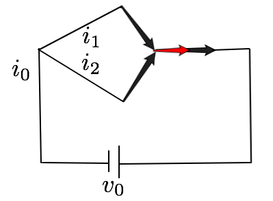

We can write an approximate (first order contribution) equation for the thermal average of the effective resistance of the form:
| (5) |
where and are two resistances which depend on the value of and the geometry of the spin ice (which is contained in ). The resistances are defined as quadratic forms (see SM-C)
| (6) |
where and , and is a circuit dependent vector. The two limiting resistances can be obtained also if the interaction is antiferromagnetic (and the graph bipartite). The smoothed theta function, in this case, is a reasonable smoothed -function is , where which incorporetates a sharp transition or a crossover. The effective mechanism is based on the fact that that the equilibrium temperature depends on the balance between radiation and current induced Joule heating. Thus, in the simplest possible approximation, we see that under the application of a small magnetic field the resistance of the material can be assumed to be a thermal phase-change type of material (or switches), in which the system has two resistance phases depending on the current, which in turn controls the temperature of the permalloy via Joule heating. If the transition is not sharp but only a crossover, then we can assume that
| (7) |
where is a smooth function such that as and and as . In this case, it seems reasonable to assume that the material will fall in the thermal memristor framework introduced in [53]. Then, because we expect the typical memristive hysteresis to be small, it is possible to see the change in the resistances from the Lissajous figures (Fig. 2), obtained from the functional dependence of the effective resistance which we have obtained.

Another mechanism for moment inversion in nanowires which does not require very careful fine tuning of the temperature, is the current-induced domain wall inversion via spin-transfer [54]. Specifically, when a current is applied to a magnetic nanowire, some domain wall defects can form at the junctions and quickly move along the wires [55, 56, 57]. This phenomenon can be effectively modeled in our system by assuming that if the current in a wire is higher than a certain threshold , then the spin along that wire is inverted.
In a large system this hard switching behavior gets smoothed out. We consider an extended Honeycomb circuit of 16 loops, where heach whire has resistence . We then consider the following two-steps spin dynamics. At each time step we start with a spin configuration , solve for the Kirchhoff laws in the nanowires, and find the equilibrium currents in the material as a function of the external voltage only. We then use the eqns derived in the SM-C to find the auxiliary voltage generators (given the spin configuration ) in the material which will affect the spin configuration . At this point, we consider the domain-wall inversion process. If the current in each wire is above a certain threshold and the current is in the opposite direction of the magnetization direction of that wire, we flip the magnetization direction instantaneously. In experiments like those of [54] the switching is extremely fast. We thus consider for simplicity instantaneous inversion.
We account for the manybody interaction among spins by imposing constraints on the possible vertex configurations. Honeycomb spin ice [52, 58, 59, 63] is frustrated and at low energy enters an ice-rule regime where only vertices with two moments pointing in and one out, or viceversa, are allowed. Therefore we only allow spin inversion when it produces vertices of magnetic charge equal to , and neglect the nodes with .
Once we fixed all the parameters, there will be a threshold which depends on the size of the system and the resistivity of the material above which the spin-inversion occurs and below which the system is a normal resistor. The threshold dynamics is reminishent of a fuse-network dynamics [64], but with the difference that it is not the conductance that dramatically drops, but that the effective voltages change instead.
In Fig. 4 we plot resultsof current vs. voltage. For small values of no memristive behavior is present (inset), as expected. For both the non-interacting (red) and interacting (blue) honeycomb lattice we obtain a zero-crossing pinched hysteresis loop typical of memristive devices and which suggests the presence of memory [41, 42, 43]. The latter is more hysteretic and smoother than the former but memristive behavior is already present even in absence of interactions. The area of hysteresis is small due to the small value of the magneto resistence effect.
We have put forward a theoretical framework for the study of memory properties of magnetic nanowires subject to an external field as an effect of anisotropic magnetoresistance, building on previous results [52]. We have derived exact and general equations which show, given a certain spin ice lattice, how the resistance of the material changes given the internal configuration. This has enabled us to obtain first order contributions to the resistance, showing that there exist an effective resistance in parallel to the nanowires network and which depends on the internal state of magnetization. Then teh coupling between current and magnetism lead to a memristive behavior. We studied two mechanisms which induce these memory effects, and which likely coexist. As the anisotropic magnetoresistance effect is of the order of a few percentages, we expect a smaller change in the value of the resistance as a function of the voltage. However, we have shown that the hysteresis curves depend on the many-body interaction and the configurational manifold of artificial spin ices. This suggests that more generally the functionality of artificial spin ice memristors can be open to design–as so many other properties of these materials proved to me. These ideas are an alternative to Spin-Torque memristors for bio-inspired computing [65], to produce an effective magnetic phase-change material [66]. In fact, because of the sensitivity to temperature, memory resistors in spin ices can have a variety of behaviors that can serve as an alternative to known Spin-Transfer-Torque devices [65, 67] and Phase-Change Materials [66]. Furthermore, as the magnetic moments can be acted upon collectively by external magnetic field, or individually, artificial spin ice memristors could be reprogrammable.
The work of FC and CN was carried out under the auspices of the US Department of Energy through the Los Alamos National Laboratory, operated by Triad National Security, LLC (Contract No. 892333218NCA000001). CN was founded by DOE-LDRD grant 2017014ER. FC was also financed via DOE-LDRD grants PRD20170660 and PRD20190195.
References
- [1] C. Nisoli et al.,Rev. Mod. Phys. 85, 1473 (2013)
- [2] R. F. Wang et al., Nature 439(7074):303-6, (2006).
- [3] S.D. Bader, Rev. Mod. Phys., 78(1):1, (2006).
- [4] I. Gilbert et al., Nature Phys. 12, 162-165 (2016)
- [5] L. J. Heyderman, R. L. Stamps, J. of Phys.: Condensed Matter, 25(36):363201 (2013)
- [6] B. Canals et al., Nat. Comm. 7 (2016)
- [7] IA Chioar, et al., Phys. Rev. B, 93(21):214410 (2016). Nature, 540(7633):410-413 (2016).
- [8] C. Nisoli et al, Phys. Rev. Lett., 98(21):217203 (2007)
- [9] C. Nisoli et al., Phys. Rev. Lett., 105(4):047205 (2010)
- [10] C. Nisoli, V. Kapaklis, P. Schiffer, Nature Phys.13(3):200-203 (2017)
- [11] I. Gilbert et al., Nat Phys. 10(9):670-675 (2014)
- [12] V. S. Bhat et al., Phys. Rev. Lett. 111(7):077201 (2013)
- [13] A. Ortiz-Ambriz, P. Tierno, Nature Comm. 7 (2016)
- [14] P. Tierno, Phys Rev. Lett. 116(3):038303 (2016)
- [15] J. Loehr, A. Ortiz-Ambriz, P. Tierno. Phys. Rev. Lett. 117(16):168001 (2016)
- [16] M. L. Latimer et al., Phys. Rev. Lett., 111:067001 (2013)
- [17] J. C. Gartside et al., Nature Nano., 13(1):53-58 (2018)
- [18] Z. Li et al.,Small 14, 1800868 (2018)
- [19] Y.-L. Wang et al., Science, 352(6288):962966, 2016.
- [20] C. Castelnovo et al.,Annu. Rev. Condens. Matter Phys., 3(1):35-55 (2012)
- [21] E. Mengotti et al., Nat. Phys., 7(1):68-74 (2010)
- [22] Y. Lao et al., Nature Phys. 14 (2009)
- [23] G.-W. Chern, P. Mellado, EPL 114 (3): 37004 (2016)
- [24] S. Gliga, et al., Phys. Rev. Lett, 110(11):117205 (2013).
- [25] I. Gilbert et al., Phys. Rev. B, 92(10):104417 (2015)
- [26] P. E. Lammert et al., Nat. Phys., 6(10):786-789 (2010)
- [27] F. Caravelli, C. Nisoli, arXiv:1810.09190
- [28] H. Arava et al, Nanotechnology 29, no. 26 265205 (2018)
- [29] J. H. Hensen, E. Folven, G. Tufte, Proc. of ALIFE 2018, pp. 15-22, MIT Press, 10.1162/isal-a-00011 (2018)
- [30] S. A. Wolf et al., Science 294(5546):1488-1495 (2001)
- [31] A. Ney et al., Nature 425(6957): 485-7 (2003)
- [32] M. Patra, S. K. Maiti, Eur. Phys. Lett. 121(38004), (2018)
- [33] Y. Zhang, IEEE in Design, Automation and Test in Europe Conference and Exhibition, 10.7873/DATE.2014.316 (2014)
- [34] F. L. Traversa et al., Science Advances 1 (6), e1500031 (2015)
- [35] F. L. Traversa, M. Di Ventra, Chaos 27, 023107 (2017)
- [36] H. Manukian et al.,IEEE Trans Neural Netw Learn Syst. (2017)
- [37] F. Traversa, M. Di Ventra, J. App. Phys.,123 (2018)
- [38] F. Caravelli, F. L. Traversa, M. Di Ventra,Phys. Rev. E 95, 022140 (2017)
- [39] F. Caravelli, Entropy 21(8), 789 (2019)
- [40] D. Ielmini, H.-S. P. Wong, Nature Electronics 1, 333-343 (2018)
- [41] M. Di Ventra, Y. V. Pershin, Nature Phys. 9, 200-202 (2013)
- [42] F. Caravelli, J. P. Carbajal, Technologies 2018, 6(4), 118; engrXiv preprint:c4qr9
- [43] D. S. Jeong et al, Adv. Electron. Mater., 2: 1600090. (2016)
- [44] T. Serrano-Gotarredona et al., Front. Neurosci. 7: 2 (2013) https://doi.org/10.3389/fnins.2013.00002
- [45] A. Imre et al., Science, 311 (5758) 205-208, (2006).
- [46] G. Csaba, et al., IEEE Trans. on Nano., 99(4), 2009 (2003)
- [47] M. Gonellia, et al., J. of Mag. and Mag. Mat. 460, 432 (2018)
- [48] M. T. Niemier et al., J. of Phys.: Condensed Matter, 23(49), 493202 (2011)
- [49] B. Le, et al. Phys. Rev. B 95, 060405(R) (2017)
- [50] T. R. McGuire and R. I. Potter,IEEE Trans. Magnetics 11, 1018 (1975).
- [51] W. R. Branford et al.,Science 335(6076), pp. 1597-1600 (2012)
- [52] G.-W. Chern, Phys. Rev. Applied 8,064006 (2017)
- [53] F. Yang, M. P. Gordon, J. J. Urban,J. of App. Phys. 125, 025109 (2019);
- [54] A. Yamaguchi et al., Phys. Rev. Lett. 92(7), 077205-4 (2004)
- [55] S. Krishnia, I. Purnama, W. S. Lew, J. Mag. Mag. Materials 420 (2016) 158-165,
- [56] N. Vernier et al, Eur. Phys. Lett. 65(526), 2004
- [57] A. Pushp et al., Nature Phys. volume 9, pages 505–511 (2013)
- [58] Y. Qi, T. Brintlinger, J. Cumings Phys. Rev. B 77, 094418 (2008)
- [59] S. Zhang et al, Nature 500, pages 553–557 (2013)
- [60] B. Bollobas, Modern Graph Theory, Springer Science, New York (1998)
- [61] F. Caravelli, Phys. Rev. E 96(5) (2017)
- [62] F. Caravelli Int. J. of Par., Em. and Dist. Sys., 33:4, pp. 350-366, (2018)
- [63] G.-W. Chern, O. Tchernyshyov,Phil. Trans. Roy. Soc. A 370, 5718 (2012)
- [64] F. C. Sheldon, M. Di Ventra, Phys. Rev. E 95(1), 2017
- [65] N. Locatelli, V. Cros, J. Grollier, Nature Materials, 13, 11 (2014)
- [66] S. Raoux, F. Xiong , M. Wuttig, E. Pop, MRS Bulletin 39, pp. 703-710 (2014)
- [67] M. Stiles, J. Miltat, B. Hillebrands, A. Thiaville (Eds.): Spin Dynamics in Confined Magnetic Structures III, Topics Appl. Physics 101, 225–308 (2006) (Springer-Verlag Berlin Heidelberg 2006)